Introduction to Microcontrollers
Introduction
History
Microcontrollers versus microprocessors
1.1 Memory unit
1.2 Central processing unit
1.3 Buses
1.4 Input-output unit
1.5 Serial communication
1.6 Timer unit
1.7 Watchdog
1.8 Analog to digital converter
1.9 Program
History
Microcontrollers versus microprocessors
1.1 Memory unit
1.2 Central processing unit
1.3 Buses
1.4 Input-output unit
1.5 Serial communication
1.6 Timer unit
1.7 Watchdog
1.8 Analog to digital converter
1.9 Program
Circumstances that we find ourselves in today in the field of microcontrollers had their beginnings in the development of technology of integrated circuits. This development has made it possible to store hundreds of thousands of transistors into one chip. That was a prerequisite for production of microprocessors , and the first computers were made by adding external peripherals such as memory, input-output lines, timers and other. Further increasing of the volume of the package resulted in creation of integrated circuits. These integrated circuits contained both processor and peripherals. That is how the first chip containing a microcomputer , or what would later be known as a microcontroller came about.
It was year 1969, and a team of Japanese engineers from the BUSICOM company arrived to United States with a request that a few integrated circuits for calculators be made using their projects. The proposition was set to INTEL, and Marcian Hoff was responsible for the project. Since he was the one who has had experience in working with a computer (PC) PDP8, it occured to him to suggest a fundamentally different solution instead of the suggested construction. This solution presumed that the function of the integrated circuit is determined by a program stored in it. That meant that configuration would be more simple, but that it would require far more memory than the project that was proposed by Japanese engineers would require. After a while, though Japanese engineers tried finding an easier solution, Marcian's idea won, and the first microprocessor was born. In transforming an idea into a ready made product , Frederico Faggin was a major help to INTEL. He transferred to INTEL, and in only 9 months had succeeded in making a product from its first conception. INTEL obtained the rights to sell this integral block in 1971. First, they bought the license from the BUSICOM company who had no idea what treasure they had. During that year, there appeared on the market a microprocessor called 4004. That was the first 4-bit microprocessor with the speed of 6 000 operations per second. Not long after that, American company CTC requested from INTEL and Texas Instruments to make an 8-bit microprocessor for use in terminals. Even though CTC gave up this idea in the end, Intel and Texas Instruments kept working on the microprocessor and in April of 1972, first 8-bit microprocessor appeard on the market under a name 8008. It was able to address 16Kb of memory, and it had 45 instructions and the speed of 300 000 operations per second. That microprocessor was the predecessor of all today's microprocessors. Intel kept their developments up in April of 1974, and they put on the market the 8-bit processor under a name 8080 which was able to address 64Kb of memory, and which had 75 instructions, and the price began at $360.
In another American company Motorola, they realized quickly what was happening, so they put out on the market an 8-bit microprocessor 6800. Chief constructor was Chuck Peddle, and along with the processor itself, Motorola was the first company to make other peripherals such as 6820 and 6850. At that time many companies recognized greater importance of microprocessors and began their own developments. Chuck Peddle leaved Motorola to join MOS Technology and kept working intensively on developing microprocessors.
At the WESCON exhibit in United States in 1975, a critical event took place in the history of microprocessors. The MOS Technology announced it was marketing microprocessors 6501 and 6502 at $25 each, which buyers could purchase immediately. This was so sensational that many thought it was some kind of a scam, considering that competitors were selling 8080 and 6800 at $179 each. As an answer to its competitor, both Intel and Motorola lowered their prices on the first day of the exhibit down to $69.95 per microprocessor. Motorola quickly brought suit against MOS Technology and Chuck Peddle for copying the protected 6800. MOS Technology stopped making 6501, but kept producing 6502. The 6502 was a 8-bit microprocessor with 56 instructions and a capability of directly addressing 64Kb of memory. Due to low cost , 6502 becomes very popular, so it was installed into computers such as: KIM-1, Apple I, Apple II, Atari, Comodore, Acorn, Oric, Galeb, Orao, Ultra, and many others. Soon appeared several makers of 6502 (Rockwell, Sznertek, GTE, NCR, Ricoh, and Comodore takes over MOS Technology) which was at the time of its prosperity sold at a rate of 15 million processors a year!
Others were not giving up though. Frederico Faggin leaves Intel, and starts his own Zilog Inc.
In 1976 Zilog announced the Z80. During the making of this microprocessor, Faggin made a pivotal decision. Knowing that a great deal of programs have been already developed for 8080, Faggin realized that many would stay faithful to that microprocessor because of great expenditure which redoing of all of the programs would result in. Thus he decided that a new processor had to be compatible with 8080, or that it had to be capable of performing all of the programs which had already been written for 8080. Beside these characteristics, many new ones have been added, so that Z80 was a very powerful microprocessor in its time. It was able to address directly 64 Kb of memory, it had 176 instructions, a large number of registers, a built in option for refreshing the dynamic RAM memory, single-supply, greater speed of work etc. Z80 was a great success and everybody converted from 8080 to Z80. It could be said that Z80 was without a doubt commercially most successful 8-bit microprocessor of that time. Besides Zilog, other new manufacturers like Mostek, NEC, SHARP, and SGS also appeared. Z80 was the heart of many computers like Spectrum, Partner, TRS703, Z-3 .
In 1976, Intel came up with an improved version of 8-bit microprocessor named 8085. However, Z80 was so much better that Intel soon lost the battle. Altough a few more processors appeared on the market (6809, 2650, SC/MP etc.), everything was actually already decided. There weren't any more great improvements to make manufacturers convert to something new, so 6502 and Z80 along with 6800 remained as main representatives of the 8-bit microprocessors of that time.
Microcontroller differs from a microprocessor in many ways. First and the most important is its functionality. In order for a microprocessor to be used, other components such as memory, or components for receiving and sending data must be added to it. In short that means that microprocessor is the very heart of the computer. On the other hand, microcontroller is designed to be all of that in one. No other external components are needed for its application because all necessary peripherals are already built into it. Thus, we save the time and space needed to construct devices.
Memory is part of the microcontroller whose function is to store data.
The easiest way to explain it is to describe it as one big closet with lots of drawers. If we suppose that we marked the drawers in such a way that they can not be confused, any of their contents will then be easily accessible. It is enough to know the designation of the drawer and so its contents will be known to us for sure.
The easiest way to explain it is to describe it as one big closet with lots of drawers. If we suppose that we marked the drawers in such a way that they can not be confused, any of their contents will then be easily accessible. It is enough to know the designation of the drawer and so its contents will be known to us for sure.
Memory components are exactly like that. For a certain input we get the contents of a certain addressed memory location and that's all. Two new concepts are brought to us: addressing and memory location. Memory consists of all memory locations, and addressing is nothing but selecting one of them. This means that we need to select the desired memory location on one hand, and on the other hand we need to wait for the contents of that location. Beside reading from a memory location, memory must also provide for writing onto it. This is done by supplying an additional line called control line. We will designate this line as R/W (read/write). Control line is used in the following way: if r/w=1, reading is done, and if opposite is true then writing is done on the memory location. Memory is the first element, and we need a few operation of our microcontroller .
Let add 3 more memory locations to a specific block that will have a built in capability to multiply, divide, subtract, and move its contents from one memory location onto another. The part we just added in is called "central processing unit" (CPU). Its memory locations are called registers.
Registers are therefore memory locations whose role is to help with performing various mathematical operations or any other operations with data wherever data can be found. Look at the current situation. We have two independent entities (memory and CPU) which are interconnected, and thus any exchange of data is hindered, as well as its functionality. If, for example, we wish to add the contents of two memory locations and return the result again back to memory, we would need a connection between memory and CPU. Simply stated, we must have some "way" through data goes from one block to another.
That "way" is called "bus". Physically, it represents a group of 8, 16, or more wires
There are two types of buses: address and data bus. The first one consists of as many lines as the amount of memory we wish to address, and the other one is as wide as data, in our case 8 bits or the connection line. First one serves to transmit address from CPU memory, and the second to connect all blocks inside the microcontroller.
There are two types of buses: address and data bus. The first one consists of as many lines as the amount of memory we wish to address, and the other one is as wide as data, in our case 8 bits or the connection line. First one serves to transmit address from CPU memory, and the second to connect all blocks inside the microcontroller.
As far as functionality, the situation has improved, but a new problem has also appeared: we have a unit that's capable of working by itself, but which does not have any contact with the outside world, or with us! In order to remove this deficiency, let's add a block which contains several memory locations whose one end is connected to the data bus, and the other has connection with the output lines on the microcontroller which can be seen as pins on the electronic component.
Those locations we've just added are called "ports". There are several types of ports : input, output or bidiectional ports. When working with ports, first of all it is necessary to choose which port we need to work with, and then to send data to, or take it from the port.
When working with it the port acts like a memory location. Something is simply being written into or read from it, and it could be noticed on the pins of the microcontroller.
Beside stated above we've added to the already existing unit the possibility of communication with an outside world. However, this way of communicating has its drawbacks. One of the basic drawbacks is the number of lines which need to be used in order to transfer data. What if it is being transferred to a distance of several kilometers? The number of lines times number of kilometers doesn't promise the economy of the project. It leaves us having to reduce the number of lines in such a way that we don't lessen its functionality. Suppose we are working with three lines only, and that one line is used for sending data, other for receiving, and the third one is used as a reference line for both the input and the output side. In order for this to work, we need to set the rules of exchange of data. These rules are called protocol. Protocol is therefore defined in advance so there wouldn't be any misunderstanding between the sides that are communicating with each other. For example, if one man is speaking in French, and the other in English, it is highly unlikely that they will quickly and effectively understand each other. Let's suppose we have the following protocol. The logical unit "1" is set up on the transmitting line until transfer begins. Once the transfer starts, we lower the transmission line to logical "0" for a period of time (which we will designate as T), so the receiving side will know that it is receiving data, and so it will activate its mechanism for reception. Let's go back now to the transmission side and start putting logic zeros and ones onto the transmitter line in the order from a bit of the lowest value to a bit of the highest value. Let each bit stay on line for a time period which is equal to T, and in the end, or after the 8th bit, let us bring the logical unit "1" back on the line which will mark the end of the transmission of one data. The protocol we've just described is called in professional literature NRZ (Non-Return to Zero).
As we have separate lines for receiving and sending, it is possible to receive and send data (info.) at the same time. So called full-duplex mode block which enables this way of communication is called a serial communication block. Unlike the parallel transmission, data moves here bit by bit, or in a series of bits what defines the term serial communication comes from. After the reception of data we need to read it from the receiving location and store it in memory as opposed to sending where the process is reversed. Data goes from memory through the bus to the sending location, and then to the receiving unit according to the protocol.
Since we have the serial communication explained, we can receive, send and process data.
However, in order to utilize it in industry we need a few additionally blocks. One of those is the timer block which is significant to us because it can give us information about time, duration, protocol etc. The basic unit of the timer is a free-run counter which is in fact a register whose numeric value increments by one in even intervals, so that by taking its value during periods T1 and T2 and on the basis of their difference we can determine how much time has elapsed. This is a very important part of the microcontroller whose understanding requires most of our time.
One more thing is requiring our attention is a flawless functioning of the microcontroller
during its run-time. Suppose that as a result of some interference (which often does occur in industry) our microcontroller stops executing the program, or worse, it starts working incorrectly.
during its run-time. Suppose that as a result of some interference (which often does occur in industry) our microcontroller stops executing the program, or worse, it starts working incorrectly.
Of course, when this happens with a computer, we simply reset it and it will keep working. However, there is no reset button we can push on the microcontroller and thus solve our problem. To overcome this obstacle, we need to introduce one more block called watchdog. This block is in fact another free-run counter where our program needs to write a zero in every time it executes correctly. In case that program gets "stuck", zero will not be written in, and counter alone will reset the microcontroller upon achieving its maximum value. This will result in executing the program again, and correctly this time around. That is an important element of every program to be reliable without man's supervision.
As the peripheral signals usually are substantially different from the ones that microcontroller can understand (zero and one), they have to be converted into a pattern which can be comprehended by a microcontroller. This task is performed by a block for analog to digital conversion or by an ADC. This block is responsible for converting an information about some analog value to a binary number and for follow it through to a CPU block so that CPU block can further process it.
Finnaly, the microcontroller is now completed, and all we need to do now is to assemble it into an electronic component where it will access inner blocks through the outside pins. The picture below shows what a microcontroller looks like inside.
Physical configuration of the interior of a microcontroller
Thin lines which lead from the center towards the sides of the microcontroller represent wires connecting inner blocks with the pins on the housing of the microcontroller so called bonding lines. Chart on the following page represents the center section of a microcontroller.
Microcontroller outline with its basic elements and internal connections
For a real application, a microcontroller alone is not enough. Beside a microcontroller, we need a program that would be executed, and a few more elements which make up a interface logic towards the elements of regulation (which will be discussed in later chapters).
Program writing is a special field of work with microcontrollers and is called "programming". Try to write a small program in a language that we will make up ourselves first and then would be understood by anyone.
START
REGISTER1=MEMORY LOCATION_A
REGISTER2=MEMORY LOCATION_B
PORTA=REGISTER1 + REGISTER2
END
The program adds the contents of two memory locations, and views their sum on port A. The first line of the program stands for moving the contents of memory location "A" into one of the registers of central processing unit. As we need the other data as well, we will also move it into the other register of the central processing unit. The next instruction instructs the central processing unit to add the contents of those two registers and send a result to port A, so that sum of that addition would be visible to the outside world. For a more complex problem, program that works on its solution will be bigger.
Programming can be done in several languages such as Assembler, C and Basic which are most commonly used languages. Assembler belongs to lower level languages that are programmed slowly, but take up the least amount of space in memory and gives the best results where the speed of program execution is concerned. As it is the most commonly used language in programming microcontrollers it will be discussed in a later chapter. Programs in C language are easier to be written, easier to be understood, but are slower in executing from assembler programs. Basic is the easiest one to learn, and its instructions are nearest a man's way of reasoning, but like C programming language it is also slower than assembler. In any case, before you make up your mind about one of these languages you need to consider carefully the demands for execution speed, for the size of memory and for the amount of time available for its assembly.
After the program is written, we would install the microcontroller into a device and run it. In order to do this we need to add a few more external components necessary for its work. First we must give life to a microcontroller by connecting it to a power supply (power needed for operation of all electronic instruments) and oscillator whose role is similar to the role that heart plays in a human body. Based on its clocks microcontroller executes instructions of a program. As it receives supply microcontroller will perform a small check up on itself, look up the beginning of the program and start executing it. How the device will work depends on many parameters, the most important of which is the skillfulness of the developer of hardware, and on programmer's expertise in getting the maximum out of the device with his program.
Microcontroller PIC16F84
Introduction
CISC, RISC
Applications
Clock/instruction cycle
Pipelining
Pin description
2.1 Clock generator - oscillator
2.2 Reset
2.3 Central processing unit
2.4 Ports
2.5 Memory organization
2.6 Interrupts
2.7 Free timer TMR0
2.8 EEPROM Data memory
Introduction
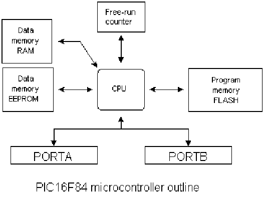
PIC16F84 belongs to a class of 8-bit microcontrollers of RISC architecture. Its general structure is shown on the following map representing basic blocks.
Program memory (FLASH)- for storing a written program.
Since memory made in FLASH technology can be programmed and cleared more than once, it makes this microcontroller suitable for device development.
EEPROM - data memory that needs to be saved when there is no supply.
It is usually used for storing important data that must not be lost if power supply suddenly stops. For instance, one such data is an assigned temperature in temperature regulators. If during a loss of power supply this data was lost, we would have to make the adjustment once again upon return of supply. Thus our device looses on self-reliance.
RAM - data memory used by a program during its execution.
In RAM are stored all inter-results or temporary data during run-time.
PORTA and PORTB are physical connections between the microcontroller and the outside world. Port A has five, and port B has eight pins.
FREE-RUN TIMER is an 8-bit register inside a microcontroller that works independently of the program. On every fourth clock of the oscillator it increments its value until it reaches the maximum (255), and then it starts counting over again from zero. As we know the exact timing between each two increments of the timer contents, timer can be used for measuring time which is very useful with some devices.
CENTRAL PROCESSING UNIT has a role of connective element between other blocks in the microcontroller. It coordinates the work of other blocks and executes the user program.
CISC, RISC
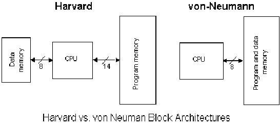
It has already been said that PIC16F84 has a RISC architecture. This term is often found in computer literature, and it needs to be explained here in more detail. Harvard architecture is a newer concept than von-Neumann's. It rose out of the need to speed up the work of a microcontroller. In Harvard architecture, data bus and address bus are separate. Thus a greater flow of data is possible through the central processing unit, and of course, a greater speed of work. Separating a program from data memory makes it further possible for instructions not to have to be 8-bit words. PIC16F84 uses 14 bits for instructions which allows for all instructions to be one word instructions. It is also typical for Harvard architecture to have fewer instructions than von-Neumann's, and to have instructions usually executed in one cycle.
Microcontrollers with Harvard architecture are also called "RISC microcontrollers". RISC stands for Reduced Instruction Set Computer. Microcontrollers with von-Neumann's architecture are called 'CISC microcontrollers'. Title CISC stands for Complex Instruction Set Computer.
Since PIC16F84 is a RISC microcontroller, that means that it has a reduced set of instructions, more precisely 35 instructions . (ex. Intel's and Motorola's microcontrollers have over hundred instructions) All of these instructions are executed in one cycle except for jump and branch instructions. According to what its maker says, PIC16F84 usually reaches results of 2:1 in code compression and 4:1 in speed in relation to other 8-bit microcontrollers in its class.
Applications
PIC16F84 perfectly fits many uses, from automotive industries and controlling home appliances to industrial instruments, remote sensors, electrical door locks and safety devices. It is also ideal for smart cards as well as for battery supplied devices because of its low consumption.
EEPROM memory makes it easier to apply microcontrollers to devices where permanent storage of various parameters is needed (codes for transmitters, motor speed, receiver frequencies, etc.). Low cost, low consumption, easy handling and flexibility make PIC16F84 applicable even in areas where microcontrollers had not previously been considered (example: timer functions, interface replacement in larger systems, coprocessor applications, etc.).
In System Programmability of this chip (along with using only two pins in data transfer) makes possible the flexibility of a product, after assembling and testing have been completed. This capability can be used to create assembly-line production, to store calibration data available only after final testing, or it can be used to improve programs on finished products.
Clock / instruction cycle
Clock is microcontroller's main starter, and is obtained from an external component called an "oscillator". If we want to compare a microcontroller with a time clock, our "clock" would then be a ticking sound we hear from the time clock. In that case, oscillator could be compared to a spring that is wound so time clock can run. Also, force used to wind the time clock can be compared to an electrical supply.
Clock from the oscillator enters a microcontroller via OSC1 pin where internal circuit of a microcontroller divides the clock into four even clocks Q1, Q2, Q3, and Q4 which do not overlap. These four clocks make up one instruction cycle (also called machine cycle) during which one instruction is executed.
Execution of instruction starts by calling an instruction that is next in string. Instruction is called from program memory on every Q1 and is written in instruction register on Q4. Decoding and execution of instruction are done between the next Q1 and Q4 cycles. On the following diagram we can see the relationship between instruction cycle and clock of the oscillator (OSC1) as well as that of internal clocks Q1-Q4. Program counter (PC) holds information about the address of the next instruction.

Pipelining
Instruction cycle consists of cycles Q1, Q2, Q3 and Q4. Cycles of calling and executing instructions are connected in such a way that in order to make a call, one instruction cycle is needed, and one more is needed for decoding and execution. However, due to pipelining, each instruction is effectively executed in one cycle. If instruction causes a change on program counter, and PC doesn't point to the following but to some other address (which can be the case with jumps or with calling subprograms), two cycles are needed for executing an instruction. This is so because instruction must be processed again, but this time from the right address. Cycle of calling begins with Q1 clock, by writing into instruction register (IR). Decoding and executing begins with Q2, Q3 and Q4 clocks.

TCY0 reads in instruction MOVLW 55h (it doesn't matter to us what instruction was executed, because there is no rectangle pictured on the bottom).
TCY1 executes instruction MOVLW 55h and reads in MOVWF PORTB.
TCY2 executes MOVWF PORTB and reads in CALL SUB_1.
TCY3 executes a call of a subprogram CALL SUB_1, and reads in instruction BSF PORTA, BIT3. As this instruction is not the one we need, or is not the first instruction of a subprogram SUB_1 whose execution is next in order, instruction must be read in again. This is a good example of an instruction needing more than one cycle.
TCY4 instruction cycle is totally used up for reading in the first instruction from a subprogram at address SUB_1.
TCY5 executes the first instruction from a subprogram SUB_1 and reads in the next one.
Pin description
PIC16F84 has a total of 18 pins. It is most frequently found in a DIP18 type of case but can also be found in SMD case which is smaller from a DIP. DIP is an abbreviation for Dual In Package. SMD is an abbreviation for Surface Mount Devices suggesting that holes for pins to go through when mounting, aren't necessary in soldering this type of a component.

Pins on PIC16F84 microcontroller have the following meaning:
Pin no.1 RA2 Second pin on port A. Has no additional function
Pin no.2 RA3 Third pin on port A. Has no additional function.
Pin no.3 RA4 Fourth pin on port A. TOCK1 which functions as a timer is also found on this pin
Pin no.4 MCLR Reset input and Vpp programming voltage of a microcontroller
Pin no.5 Vss Ground of power supply.
Pin no.6 RB0 Zero pin on port B. Interrupt input is an additional function.
Pin no.7 RB1 First pin on port B. No additional function.
Pin no.8 RB2 Second pin on port B. No additional function.
Pin no.9 RB3 Third pin on port B. No additional function.
Pin no.10 RB4 Fourth pin on port B. No additional function.
Pin no.11 RB5 Fifth pin on port B. No additional function.
Pin no.12 RB6 Sixth pin on port B. 'Clock' line in program mode.
Pin no.13 RB7 Seventh pin on port B. 'Data' line in program mode.
Pin no.14 Vdd Positive power supply pole.
Pin no.15 OSC2 Pin assigned for connecting with an oscillator
Pin no.16 OSC1 Pin assigned for connecting with an oscillator
Pin no.17 RA2 Second pin on port A. No additional function
Pin no.18 RA1 First pin on port A. No additional function.
2.1 Clock generator - oscillator
Oscillator circuit is used for providing a microcontroller with a clock. Clock is needed so that microcontroller could execute a program or program instructions.
Types of oscillators
PIC16F84 can work with four different configurations of an oscillator. Since configurations with crystal oscillator and resistor-capacitor (RC) are the ones that are used most frequently, these are the only ones we will mention here. Microcontroller type with a crystal oscillator has in its designation XT, and a microcontroller with resistor-capacitor pair has a designation RC. This is important because you need to mention the type of oscillator when buying a microcontroller.
XT Oscillator
RC Oscillator
In applications where great time precision is not necessary, RC oscillator offers additional savings during purchase. Resonant frequency of RC oscillator depends on supply voltage rate, resistance R, capacity C and working temperature. It should be mentioned here that resonant frequency is also influenced by normal variations in process parameters, by tolerance of external R and C components, etc.
In applications where great time precision is not necessary, RC oscillator offers additional savings during purchase. Resonant frequency of RC oscillator depends on supply voltage rate, resistance R, capacity C and working temperature. It should be mentioned here that resonant frequency is also influenced by normal variations in process parameters, by tolerance of external R and C components, etc.
Above diagram shows how RC oscillator is connected with PIC16F84. With value of resistor R being below 2.2k, oscillator can become unstable, or it can even stop the oscillation. With very high value of R (ex.1M) oscillator becomes very sensitive to noise and humidity. It is recommended that value of resistor R should be between 3 and 100k. Even though oscillator will work without an external capacitor (C=0pF), capacitor above 20pF should still be used for noise and stability. No matter which oscillator is being used, in order to get a clock that microcontroller works upon, a clock of the oscillator must be divided by 4. Oscillator clock divided by 4 can also be obtained on OSC2/CLKOUT pin, and can be used for testing or synchronizing other logical circuits.
Following a supply, oscillator starts oscillating. Oscillation at first has an unstable period and amplitude, but after some period of time it becomes stabilized.
To prevent such inaccurate clock from influencing microcontroller's performance, we need to keep the microcontroller in reset state during stabilization of oscillator's clock. Diagram above shows a typical shape of a signal which microcontroller gets from the quartz oscillator.
Chapter 2.2 Reset
Reset is used for putting the microcontroller into a 'known' condition. That practically means that microcontroller can behave rather inaccurately under certain undesirable conditions. In order to continue its proper functioning it has to be reset, meaning all registers would be placed in a starting position. Reset is not only used when microcontroller doesn't behave the way we want it to, but can also be used when trying out a device as an interrupt in program execution, or to get a microcontroller ready when loading a program.
| In order to prevent from bringing a logical zero to MCLR pin accidentally (line above it means that reset is activated by a logical zero), MCLR has to be connected via resistor to the positive supply pole. Resistor should be between 5 and 10K. This kind of resistor whose function is to keep a certain line on a logical one as a preventive, is called a pull up. | |
![clip_image001[4] clip_image001[4]](https://blogger.googleusercontent.com/img/b/R29vZ2xl/AVvXsEhtbDigpZFSYAUIDiit1n7Du1MNEOETckxjsE31bXNcHhDS5SX8q4TY9umggJ5a165oathiy7vjhFcI7mXcHg_sJDnJ2TB9xULBmXXDaYzekE6pxvRPfaRS_OBMDEZR33XipPrUD2Z_4v4/?imgmax=800)
Microcontroller PIC16F84 knows several sources of resets:
a) Reset during power on, POR (Power-On Reset)
b) Reset during regular work by bringing logical zero to MCLR microcontroller's pin.
c) Reset during SLEEP regime
d) Reset at watchdog timer (WDT) overflow
e) Reset during at WDT overflow during SLEEP work regime.
The most important reset sources are a) and b). The first one occurs each time a power supply is brought to the microcontroller and serves to bring all registers to a starting position initial state. The second one is a product of purposeful bringing in of a logical zero to MCLR pin during normal operation of the microcontroller. This second one is often used in program development.
During a reset, RAM memory locations are not being reset. They are unknown during a power up and are not changed at any reset. Unlike these, SFR registers are reset to a starting position initial state. One of the most important effects of a reset is setting a program counter (PC) to zero (0000h) , which enables the program to start executing from the first written instruction.
Reset at supply voltage drop below the permissible (Brown-out Reset)
Impulse for resetting during voltage voltage-up is generated by microcontroller itself when it detects an increase in supply Vdd (in a range from 1.2V to 1.8V). That impulse lasts 72ms which is enough time for an oscillator to get stabilized. These 72ms are provided by an internal PWRT timer which has its own RC oscillator. Microcontroller is in a reset mode as long as PWRT is active. However, as device is working, problem arises when supply doesn't drop to zero but falls below the limit that guarantees microcontroller's proper functioning. This is a likely case in practice, especially in industrial environment where disturbances and instability of supply are an everyday occurrence. To solve this problem we need to make sure that microcontroller is in a reset state each time supply falls below the approved limit.
If, according to electrical specification, internal reset circuit of a microcontroller can not satisfy the needs, special electronic components can be used which are capable of generating the desired reset signal. Beside this function, they can also function in watching over supply voltage. If voltage drops below specified level, a logical zero would appear on MCLR pin which holds the microcontroller in reset state until voltage is not within limits that guarantee accurate performance.
2.3 Central Processing Unit of a PIC microcontroller
Central processing unit (CPU) is the brain of a microcontroller. That part is responsible for finding and fetching the right instruction which needs to be executed, for decoding that instruction, and finally for its execution.
Central processing unit connects all parts of the microcontroller into one whole. Surely, its most important function is to decode program instructions. When programmer writes a program, instructions have a clear form like MOVLW 0x20. However, in order for a microcontroller to understand that, this 'letter' form of an instruction must be translated into a series of zeros and ones which is called an 'opcode'. This transition from a letter to binary form is done by translators such as assembler translator (also known as an assembler). Instruction thus fetched from program memory must be decoded by a central processing unit. We can then select from the table of all the instructions a set of actions which execute a assigned task defined by instruction. As instructions may within themselves contain assignments which require different transfers of data from one memory into another, from memory onto ports, or some other calculations, CPU must be connected with all parts of the microcontroller. This is made possible through a data bus and an address bus.
Arithmetic logic unit is responsible for performing operations of adding, subtracting, moving (left or right within a register) and logic operations. Moving data inside a register is also known as 'shifting'. PIC16F84 contains an 8-bit arithmetic logic unit and 8-bit work registers.
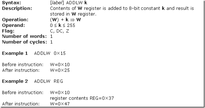
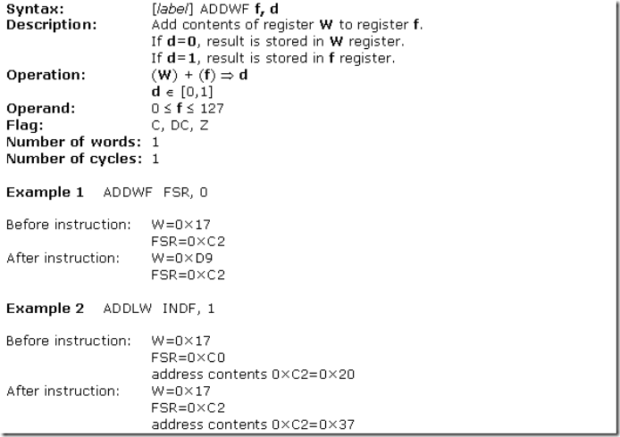
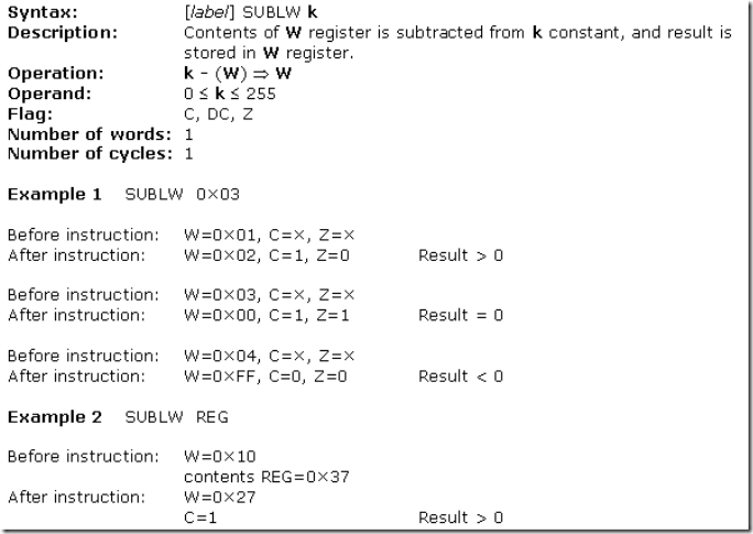
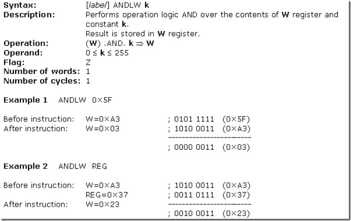
In instructions with two operands, ordinarily one operand is in work register (W register), and the other is one of the registers or a constant. By operand we mean the contents on which some operation is being done, and a register is any one of the GPR or SFR registers. GPR is an abbreviation for 'General Purposes Registers', and SFR for 'Special Function Registers'. In instructions with one operand, an operand is either W register or one of the registers. As an addition in doing operations in arithmetic and logic, ALU controls status bits (bits found in STATUS register). Execution of some instructions affects status bits, which depends on the result itself. Depending on which instruction is being executed, ALU can affect values of Carry (C), Digit Carry (DC), and Zero (Z) bits in STATUS register.
STATUS Register
bit 7 IRP (Register Bank Select bit)
Bit whose role is to be an eighth bit for purposes of indirect addressing the internal RAM.
1 = bank 2 and 3
0 = bank 0 and 1 (from 00h to FFh)
Bit whose role is to be an eighth bit for purposes of indirect addressing the internal RAM.
1 = bank 2 and 3
0 = bank 0 and 1 (from 00h to FFh)
bits 6:5 RP1:RP0 (Register Bank Select bits)
These two bits are upper part of the address for direct addressing. As instructions which address the memory directly have only seven bits, they need one more bit in order to address all 256 bytes which is how many bytes PIC16F84 has. RP1 bit is not used, but is left for some future expansions of this microcontroller.
01 = first bank
00 = zero bank
bit 4 TO Time-out ; Watchdog overflow.
Bit is set after turning on the supply and execution of CLRWDT and SLEEP instructions. Bit is reset when watchdog gets to the end signaling that overflow took place.
1 = overflow did not occur
0 = overflow did occur
Bit is set after turning on the supply and execution of CLRWDT and SLEEP instructions. Bit is reset when watchdog gets to the end signaling that overflow took place.
1 = overflow did not occur
0 = overflow did occur
bit 3 PD (Power-down bit)
This bit is set whenever power supply is brought to a microcontroller : as it starts running, after each regular reset and after execution of instruction CLRWDT. Instruction SLEEP resets it when microcontroller falls into low consumption mode. Its repeated setting is possible via reset or by turning the supply off/on . Setting can be triggered also by a signal on RB0/INT pin, change on RB port, upon writing to internal DATA EEPROM, and by a Watchdog.
1 = after supply has been turned on
0 = executing SLEEP instruction
bit 2 Z (Zero bit) Indication of a zero result
This bit is set when the result of an executed arithmetic or logic operation is zero.
1 = result equals zero
0 = result does not equal zero
This bit is set when the result of an executed arithmetic or logic operation is zero.
1 = result equals zero
0 = result does not equal zero
bit 1 DC (Digit Carry) DC Transfer
Bit affected by operations of addition, subtraction. Unlike C bit, this bit represents transfer from the fourth resulting place. It is set in case of subtracting smaller from greater number and is reset in the other case.
1 = transfer occurred on the fourth bit according to the order of the result
0 = transfer did not occur
DC bit is affected by ADDWF, ADDLW, SUBLW, SUBWF instructions.
bit 0 C (Carry) Transfer
Bit that is affected by operations of addition, subtraction and shifting.
1 = transfer occurred from the highest resulting bit
0 = transfer did not occur
C bit is affected by ADDWF, ADDLW, SUBLW, SUBWF instructions.
Bit that is affected by operations of addition, subtraction and shifting.
1 = transfer occurred from the highest resulting bit
0 = transfer did not occur
C bit is affected by ADDWF, ADDLW, SUBLW, SUBWF instructions.
2.5 Memory organization of a PIC microcontroller
PIC16F84 has two separate memory blocks, one for data and the other for program. EEPROM memory with GPR and SFR registers in RAM memory make up the data block, while FLASH memory makes up the program block.
Program memory
Program memory has been carried out in FLASH technology which makes it possible to program a microcontroller many times before it's installed into a device, and even after its installment if eventual changes in program or process parameters should occur. The size of program memory is 1024 locations with 14 bits width where locations zero and four are reserved for reset and interrupt vector.
Data memory
Data memory consists of EEPROM and RAM memories. EEPROM memory consists of 64 eight bit locations whose contents is not lost during loosing of power supply. EEPROM is not directly addressable, but is accessed indirectly through EEADR and EEDATA registers. As EEPROM memory usually serves for storing important parameters (for example, of a given temperature in temperature regulators) , there is a strict procedure for writing in EEPROM which must be followed in order to avoid accidental writing. RAM memory for data occupies space on a memory map from location 0x0C to 0x4F which comes to 68 locations. Locations of RAM memory are also called GPR registers which is an abbreviation for General Purpose Registers. GPR registers can be accessed regardless of which bank is selected at the moment.
SFR registers
Registers which take up first 12 locations in banks 0 and 1 are registers of specialized function assigned with certain blocks of the microcontroller. These are called Special Function Registers.
Memory Banks
Beside this 'length' division to SFR and GPR registers, memory map is also divided in 'width' (see preceding map) to two areas called 'banks'. Selecting one of the banks is done via RP0 bit in STATUS register.
Example:
bcf STATUS, RP0
Instruction BCF clears bit RP0 (RP0=0) in STATUS register and thus sets up bank 0.
bsf STATUS, RP0
Instruction BSF sets the bit RP0 (RP0=1) in STATUS register and thus sets up bank1.
It is useful to consider what would happen if the wrong bank was selected. Let's assume that we have selected bank 0 at the beginning of the program, and that we now want to write to certain register located in bank 1, say TRISB. Although we specified the name of the register TRISB, data will be actually stored to a bank 0 register at the appropriate address, which is PORTB in our example.
BANK0 macro
Bcf STATUS, RP0 ;Select memory bank 0
endm
BANK1 macro
Bsf STATUS, RP0 ;Select memory bank 1
endm
Bcf STATUS, RP0 ;Select memory bank 0
endm
BANK1 macro
Bsf STATUS, RP0 ;Select memory bank 1
endm
Bank selection can be also made via directive banksel after which name of the register to be accessed is specified. In this manner, there is no need to memorize which register is in which bank.
| Locations 0Ch - 4Fh are general purpose registers (GPR) which are used as RAM memory. When locations 8Ch - CFh in Bank 1 are accessed, we actually access the exact same locations in Bank 0. In other words , whenever you wish to access one of the GPR registers, there is no need to worry about which bank we are in! |
Program Counter
Program counter (PC) is a 13-bit register that contains the address of the instruction being executed. It is physically carried out as a combination of a 5-bit register PCLATH for the five higher bits of the address, and the 8-bit register PCL for the lower 8 bits of the address.
Program counter (PC) is a 13-bit register that contains the address of the instruction being executed. It is physically carried out as a combination of a 5-bit register PCLATH for the five higher bits of the address, and the 8-bit register PCL for the lower 8 bits of the address.
By its incrementing or change (i.e. in case of jumps) microcontroller executes program instructions step-by-step.
Stack
PIC16F84 has a 13-bit stack with 8 levels, or in other words, a group of 8 memory locations, 13 bits wide, with special purpose. Its basic role is to keep the value of program counter after a jump from the main program to an address of a subprogram . In order for a program to know how to go back to the point where it started from, it has to return the value of a program counter from a stack. When moving from a program to a subprogram, program counter is being pushed onto a stack (example of this is CALL instruction). When executing instructions such as RETURN, RETLW or RETFIE which were executed at the end of a subprogram, program counter was taken from a stack so that program could continue where was stopped before it was interrupted. These operations of placing on and taking off from a program counter stack are called PUSH and POP, and are named according to similar instructions on some bigger microcontrollers.
In System Programming
In order to program a program memory, microcontroller must be set to special working mode by bringing up MCLR pin to 13.5V, and supply voltage Vdd has to be stabilized between 4.5V to 5.5V. Program memory can be programmed serially using two 'data/clock' pins which must previously be separated from device lines, so that errors wouldn't come up during programming.
Addressing modes
RAM memory locations can be accessed directly or indirectly.
Direct Addressing
Direct Addressing is done through a 9-bit address. This address is obtained by connecting 7th bit of direct address of an instruction with two bits (RP1, RP0) from STATUS register as is shown on the following picture. Any access to SFR registers is an example of direct addressing.
Bsf STATUS, RP0 ;Bankl
movlw 0xFF ;w=0xFF
movwf TRISA ;address of TRISA register is taken from
;instruction movwf
movlw 0xFF ;w=0xFF
movwf TRISA ;address of TRISA register is taken from
;instruction movwf
Direct addressing
Indirect Addressing
Indirect unlike direct addressing does not take an address from an instruction but derives it from IRP bit of STATUS and FSR registers. Addressed location is accessed via INDF register which in fact holds the address indicated by a FSR. In other words, any instruction which uses INDF as its register in reality accesses data indicated by a FSR register. Let's say, for instance, that one general purpose register (GPR) at address 0Fh contains a value of 20. By writing a value of 0Fh in FSR register we will get a register indicator at address 0Fh, and by reading from INDF register, we will get a value of 20, which means that we have read from the first register its value without accessing it directly (but via FSR and INDF). It appears that this type of addressing does not have any advantages over direct addressing, but certain needs do exist during programming which can be solved smoothly only through indirect addressing.
Indirect unlike direct addressing does not take an address from an instruction but derives it from IRP bit of STATUS and FSR registers. Addressed location is accessed via INDF register which in fact holds the address indicated by a FSR. In other words, any instruction which uses INDF as its register in reality accesses data indicated by a FSR register. Let's say, for instance, that one general purpose register (GPR) at address 0Fh contains a value of 20. By writing a value of 0Fh in FSR register we will get a register indicator at address 0Fh, and by reading from INDF register, we will get a value of 20, which means that we have read from the first register its value without accessing it directly (but via FSR and INDF). It appears that this type of addressing does not have any advantages over direct addressing, but certain needs do exist during programming which can be solved smoothly only through indirect addressing.
Indirect addressing is very convenient for manipulating data arrays located in GPR registers. In this case, it is necessary to initialize FSR register with a starting address of the array, and the rest of the data can be accessed by incrementing the FSR register.
Such examples include sending a set of data via serial communication, working with buffers and indicators (which will be discussed further in a chapter with examples), or erasing a part of RAM memory (16 locations) as in the following instance.
Reading data from INDF register when the contents of FSR register is equal to zero returns the value of zero, and writing to it results in NOP operation (no operation).
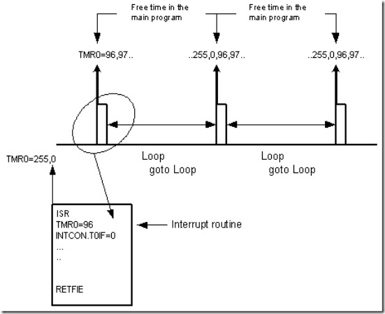
| 2.6 Interrupts Interrupts are a mechanism of a microcontroller which enables it to respond to some events at the moment they occur, regardless of what microcontroller is doing at the time. This is a very important part, because it provides connection between a microcontroller and environment which surrounds it. Generally, each interrupt changes the program flow, interrupts it and after executing an interrupt subprogram (interrupt routine) it continues from that same point on.  One of the possible sources of interrupt and how it affects the main program Control register of an interrupt is called INTCON and can be accessed regardless of the bank selected. Its role is to allow or disallowed interrupts, and in case they are not allowed, it registers single interrupt requests through its own bits. INTCON Register  Bit 7 GIE (Global Interrupt Enable bit) Bit which enables or disables all interrupts. 1 = all interrupts are enabled 0 = all interrupts are disabled Bit 6 EEIE (EEPROM Write Complete Interrupt Enable bit) Bit which enables an interrupt at the end of a writing routine to EEPROM 1 = interrupt enabled 0 = interrupt disabled If EEIE and EEIF (which is in EECON1 register) are set simultaneously , an interrupt will occur. bit 5 T0IE (TMR0 Overflow Interrupt Enable bit) Bit which enables interrupts during counter TMR0 overflow. 1 = interrupt enabled 0 = interrupt disabled If T0IE and T0IF are set simultaneously, interrupt will occur. bit 4 INTE (INT External Interrupt Enable bit) Bit which enables external interrupt from pin RB0/INT. 1 = external interrupt enabled 0 = external interrupt disabled If INTE and INTF are set simultaneously, an interrupt will occur. bit 3 RBIE (RB port change Interrupt Enable bit) Enables interrupts to occur at the change of status of pins 4, 5, 6, and 7 of port B. 1 = enables interrupts at the change of status 0 =interrupts disabled at the change of status If RBIE and RBIF are simultaneously set, an interrupt will occur. bit 2 T0IF (TMR0 Overflow Interrupt Flag bit) Overflow of counter TMR0. 1 = counter changed its status from FFh to 00h 0 = overflow did not occur Bit must be cleared in program in order for an interrupt to be detected. bit 1 INTF (INT External Interrupt Flag bit) External interrupt occurred. 1 = interrupt occurred 0 = interrupt did not occur If a rising or falling edge was detected on pin RB0/INT, (which is defined with bit INTEDG in OPTION register), bit INTF is set. bit 0 RBIF (RB Port Change Interrupt Flag bit) Bit which informs about changes on pins 4, 5, 6 and 7 of port B. 1 = at least one pin has changed its status 0 = no change occurred on any of the pins Bit has to be cleared in an interrupt subroutine to be able to detect further interrupts.  PIC16F84 has four interrupt sources: 1. Termination of writing data to EEPROM 2. TMR0 interrupt caused by timer overflow 3. Interrupt during alteration on RB4, RB5, RB6 and RB7 pins of port B. 4. External interrupt from RB0/INT pin of microcontroller Generally speaking, each interrupt source has two bits joined to it. One enables interrupts, and the other detects when interrupts occur. There is one common bit called GIE which can be used to disallow or enable all interrupts simultaneously. This bit is very useful when writing a program because it allows for all interrupts to be disabled for a period of time, so that execution of some important part of a program would not be interrupted. When instruction which resets GIE bit was executed (GIE=0, all interrupts disallowed), any interrupt that remained unsolved should be ignored. Interrupts which remained unsolved and were ignored, are processed when GIE bit (GIE=1, all interrupts allowed) would be cleared. When interrupt was answered, GIE bit was cleared so that any additional interrupts would be disabled, return address was pushed onto stack and address 0004h was written in program counter - only after this does replying to an interrupt begin! After interrupt is processed, bit whose setting caused an interrupt must be cleared, or interrupt routine would automatically be processed over again during a return to the main program. Keeping the contents of important registers Only return value of program counter is stored on a stack during an interrupt (by return value of program counter we mean the address of the instruction which was to be executed, but wasn't because interrupt occurred). Keeping only the value of program counter is often not enough. Some registers which are already in use in the main program can also be in use in interrupt routine. If they were not retained, main program would during a return from an interrupt routine get completely different values in those registers, which would cause an error in the program. One example for such a case is contents of the work register W. If we suppose that main program was using work register W for some of its operations, and if it had stored in it some value that's important for the following instruction, then an interrupt which occurs before that instruction would change the value of work register W which would directly be influenced the main program. Procedure of recording important registers before going to an interrupt routine is called PUSH, while the procedure which brings recorded values back, is called POP. PUSH and POP are instructions with some other microcontrollers (Intel), but are so widely accepted that a whole operation is named after them. PIC16F84 does not have instructions like PUSH and POP, and they have to be programmed.  Common error: saving the value wasn't done before entering the interrupt routine Due to simplicity and frequent usage, these parts of the program can be made as macros. The concept of a Macro is explained in "Program assembly language". In the following example, contents of W and STATUS registers are stored in W_TEMP and STATUS_TEMP variables prior to interrupt routine. At the beginning of PUSH routine we need to check presently selected bank because W_TEMP and STATUS_TEMP are found in bank 0. For exchange of data between these registers, SWAPF instruction is used instead of MOVF because it does not affect the STATUS register bits. Example is an assembler program for following steps: 1. Testing the current bank 2. Storing W register regardless of the current bank 3. Storing STATUS register in bank 0. 4. Executing interrupt routine for interrupt processing (ISR) 5. Restores STATUS register 6. Restores W register If there are some more variables or registers that need to be stored, then they need to be kept after storing STATUS register (step 3), and brought back before STATUS register is restored (step 5).  The same example can be carried out using macros, thus getting a more legible program. Macros that are already defined can be used for writing new macros. Macros BANK1 and BANK0 which are explained in "Memory organization" chapter are used with macros 'push' and 'pop'.  External interrupt on RB0/INT pin of microcontroller External interrupt on RB0/INT pin is triggered by rising signal edge (if bit INTEDG=1 in OPTION<6> register), or falling edge (if INTEDG=0). When correct signal appears on INT pin, INTF bit is set in INTCON register. INTF bit (INTCON<1>) must be cleared in interrupt routine, so that interrupt wouldn't occur again while going back to the main program. This is an important part of the program which programmer must not forget, or program will constantly go into interrupt routine. Interrupt can be turned off by resetting INTE control bit (INTCON<4>). Possible application of this interrupt could be measuring the impulse width or pause length, i.e. input signal frequency. Impulse duration can be measured by first enabling the interrupt on rising edge, and upon its appearing, starting the timer and then enabling the interrupt on falling edge. Timer should be stopped upon the appearing of falling edge - measured time period represents the impulse duration. Interrupt during a TMR0 counter overflow Overflow of TMR0 counter (from FFh to 00h) will set T0IF (INTCON<2>) bit. This is very important interrupt because many real problems can be solved using this interrupt. One of the examples is time measurement. If we know how much time counter needs in order to complete one cycle from 00h to FFh, then a number of interrupts multiplied by that amount of time will yield the total of elapsed time. In interrupt routine some variable would be incremented in RAM memory, value of that variable multiplied by the amount of time the counter needs to count through a whole cycle, would yield total elapsed time. Interrupt can be turned on/off by setting/resetting T0IE (INTCON<5>) bit. Interrupt upon a change on pins 4, 5, 6 and 7 of port B Change of input signal on PORTB <7:4> sets RBIF (INTCON<0>) bit. Four pins RB7, RB6, RB5 and RB4 of port B, can trigger an interrupt which occurs when status on them changes from logic one to logic zero, or vice versa. For pins to be sensitive to this change, they must be defined as input. If any one of them is defined as output, interrupt will not be generated at the change of status. If they are defined as input, their current state is compared to the old value which was stored at the last reading from port B. Interrupt upon finishing write-subroutine to EEPROM This interrupt is of practical nature only. Since writing to one EEPROM location takes about 10ms (which is a long time in the notion of a microcontroller), it doesn't pay off to a microcontroller to wait for writing to end. Thus interrupt mechanism is added which allows the microcontroller to continue executing the main program, while writing in EEPROM is being done in the background. When writing is completed, interrupt informs the microcontroller that writing has ended. EEIF bit, through which this informing is done, is found in EECON1 register. Occurrence of an interrupt can be disabled by resetting the EEIE bit in INTCON register. Interrupt initialization In order to use an interrupt mechanism of a microcontroller, some preparatory tasks need to be performed. These procedures are in short called "initialization". By initialization we define to what interrupts the microcontroller will respond, and which ones it will ignore. If we do not set the bit that allows a certain interrupt, program will not execute an interrupt subprogram. Through this we can obtain control over interrupt occurrence, which is very useful.  The above example shows initialization of external interrupt on RB0 pin of a microcontroller. Where we see one being set, that means that interrupt is enabled. Occurrence of other interrupts is not allowed, and interrupts are disabled altogether until GIE bit is set to one. The following example shows a typical way of handling interrupts. PIC16F84 has got a single location for storing the address of an interrupt subroutine. This means that first we need to detect which interrupt is at hand (if more than one interrupt source is available), and then we can execute that part of a program which refers to that interrupt. 
|
2.7 Free-run timer TMR0
Timers are usually the most complicated parts of a microcontroller, so it is necessary to set aside more time for understanding them thoroughly. Through their application it is possible to establish relations between a real dimension such as "time" and a variable which represents status of a timer within a microcontroller. Physically, timer is a register whose value is continually increasing to 255, and then it starts all over again: 0, 1, 2, 3, 4...255....0,1, 2, 3......etc.

This incrementing is done in the background of everything a microcontroller does. It is up to programmer to think up a way how he will take advantage of this characteristic for his needs. One of the ways is increasing some variable on each timer overflow. If we know how much time a timer needs to make one complete round, then multiplying the value of a variable by that time will yield the total amount of elapsed time.
PIC16F84 has an 8-bit timer. Number of bits determines what value timer counts to before starting to count from zero again. In the case of an 8-bit timer, that number is 256. A simplified scheme of relation between a timer and a prescaler is represented on the previous diagram. Prescaler is a name for the part of a microcontroller which divides oscillator clock before it will reach logic that increases timer status. Number which divides a clock is defined through first three bits in OPTION register. The highest divisor is 256. This actually means that only at every 256th clock, timer value would increase by one. This provides us with the ability to measure longer timer periods.

After each count up to 255, timer resets its value to zero and starts with a new cycle of counting to 255. During each transition from 255 to zero, T0IF bit in INTCOM register is set. If interrupts are allowed to occur, this can be taken advantage of in generating interrupts and in processing interrupt routine. It is up to programmer to reset T0IF bit in interrupt routine, so that new interrupt, or new overflow could be detected. Beside the internal oscillator clock, timer status can also be increased by the external clock on RA4/TOCKI pin. Choosing one of these two options is done in OPTION register through T0CS bit. If this option of external clock was selected, it would be possible to define the edge of a signal (rising or falling), on which timer would increase its value.

In practice, one of the typical example that is solved via external clock and a timer is counting full turns of an axis of some production machine, like transformer winder for instance. Let's wind four metal screws on the axis of a winder. These four screws will represent metal convexity. Let's place now the inductive sensor at a distance of 5mm from the head of a screw. Inductive sensor will generate the falling signal every time the head of the screw is parallel with sensor head. Each signal will represent one fourth of a full turn, and the sum of all full turns will be found in TMR0 timer. Program can easily read this data from the timer through a data bus.
The following example illustrates how to initialize timer to signal falling edges from external clock source with a prescaler 1:4. Timer works in "polig" mode.

The same example can be carried out through an interrupt in the following way:

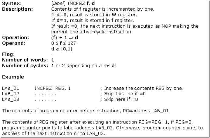
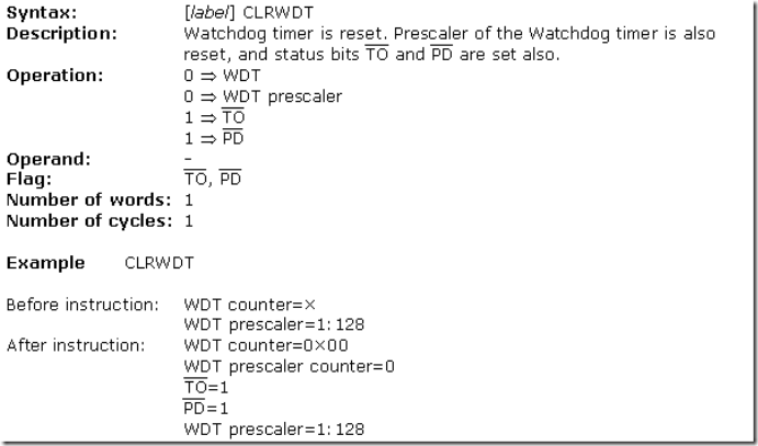
Prescaler can be assigned either timer TMR0 or a watchdog. Watchdog is a mechanism which microcontroller uses to defend itself against programs getting stuck. As with any other electrical circuit, so with a microcontroller too can occur failure, or some work impairment. Unfortunately, microcontroller also has program where problems can occur as well. When this happens, microcontroller will stop working and will remain in that state until someone resets it. Because of this, watchdog mechanism has been introduced. After a certain period of time, watchdog resets the microcontroller (microcontroller in fact resets itself). Watchdog works on a simple principle: if timer overflow occurs, microcontroller is reset, and it starts executing a program all over again. In this way, reset will occur in case of both correct and incorrect functioning. Next step is preventing reset in case of correct functioning, which is done by writing zero in WDT register (instruction CLRWDT) every time it nears its overflow. Thus program will prevent a reset as long as it's executing correctly. Once it gets stuck, zero will not be written, overflow of WDT timer and a reset will occur which will bring the microcontroller back to correct functioning again.
Prescaler is accorded to timer TMR0, or to watchdog timer trough PSA bit in OPTION register. By clearing PSA bit, prescaler will be accorded to timer TMR0. When prescaler is accorded to timer TMR0, all instructions of writing to TMR0 register (CLRF TMR0, MOVWF TMR0, BSF TMR0,...) will clear prescaler. When prescaler is assigned to a watchdog timer, only CLRWDT instruction will clear a prescaler and watchdog timer at the same time . Prescaler change is completely under programmer's control, and can be changed while program is running.
| There is only one prescaler and one timer. Depending on the needs, they are assigned either to timer TMR0 or to a watchdog. |

bit 7 RBPU (PORTB Pull-up Enable bit)
This bit turns internal pull-up resistors on port B on or off.
1 = 'pull-up' resistors turned on
0 = 'pull-up' resistors turned off
bit 6 INTEDG (Interrupt Edge Select bit)
If occurrence of interrupts was enabled, this bit would determine at what edge interrupt on RB0/INT pin would occur.
1 = rising edge
0 = falling edge
bit 5 T0CS (TMR0 Clock Source Select bit)
This pin enables a free-run timer to increment its value either from an internal oscillator, i.e. every 1/4 of oscillator clock, or via external impulses on RA4/T0CKI pin.
1 = external impulses
0 = 1/4 internal clock
bit 4 T0SE (TMR0 Source Edge Select bit)
If trigger TMR0 was enabled with impulses from a RA4/T0CKI pin, this bit would determine whether it would be on the rising or falling edge of a signal.
1 = falling edge
0 = rising edge
bit 3 PSA (Prescaler Assignment bit)
Bit which assigns prescaler between TMR0 and watchdog timer.
1 = prescaler is assigned to watchdog timer.
0 = prescaler is assigned to free timer TMR0
Bit 0:2 PS0, PS1, PS2 (Prescaler Rate Select bit)
In case of 4MHz oscillator, one instruction cycle (4 internal clocks) lasts 1µs. Numbers in the following table show the time period in µs between incrementing TMR or WDT.

2.8 EEPROM Data memory in PIC microcontrollers
PIC16F84 has 64 bytes of EEPROM memory locations on addresses from 00h to 63h that can be written to or read from. The most important characteristic of this memory is that it does not lose its contents with the loss of power supply. Data can be retained in EEPROM without power supply for up to 40 years (as manufacturer of PIC16F84 microcontroller states), and up to 1 million cycles of writing can be executed.
In practice, EEPROM memory is used for storing important data or process parameters.
One such parameter is a given temperature, assigned when setting up a temperature regulator to some process. If that data wasn't retained, it would be necessary to adjust a given temperature after each loss of supply. Since this is very impractical (and even dangerous), manufacturers of microcontrollers have began installing one smaller type of EEPROM memory.
EEPROM memory is placed in a special memory space and can be accessed through special registers. These registers are:
| EEDATA | Holds read data or that to be written. |
| EEADR | Contains an address of EEPROM location being accessed. |
| EECON1 | Contains control bits. |
| EECON2 | This register does not exist physically and serves to protect EEPROM from accidental writing. |
EECON1 register is a control register with five implemented bits. Bits 5, 6 and 7 are not used, and by reading always are zero. Interpretation of EECON1 register bits follows.
EECON1 Register
EECON1 Register
bit 4 EEIF (EEPROM Write Operation Interrupt Flag bit) Bit used to inform that writing data to EEPROM has ended.
When writing has terminated, this bit would be set automatically. Programmer must clear EEIF bit in his program in order to detect new termination of writing.
1 = writing terminated
0 = writing not terminated yet, or has not started
When writing has terminated, this bit would be set automatically. Programmer must clear EEIF bit in his program in order to detect new termination of writing.
1 = writing terminated
0 = writing not terminated yet, or has not started
bit 3 WRERR (Write EEPROM Error Flag) Error during writing to EEPROM
This bit was set only in cases when writing to EEPROM had been interrupted by a reset signal or by running out of time in watchdog timer (if activated).
1 = error occurred
0 = error did not occur
This bit was set only in cases when writing to EEPROM had been interrupted by a reset signal or by running out of time in watchdog timer (if activated).
1 = error occurred
0 = error did not occur
bit 2 WREN (EEPROM Write Enable bit) Enables writing to EEPROM
If this bit was not set, microcontroller would not allow writing to EEPROM.
1 = writing allowed
0 = writing disallowed
If this bit was not set, microcontroller would not allow writing to EEPROM.
1 = writing allowed
0 = writing disallowed
bit 1 WR (Write Control bit)
Setting of this bit initializes writing data from EEDATA register to the address specified trough EEADR register.
1 = initializes writing
0 = does not initialize writing
Setting of this bit initializes writing data from EEDATA register to the address specified trough EEADR register.
1 = initializes writing
0 = does not initialize writing
bit 0 RD (Read Control bit)
Setting this bit initializes transfer of data from address defined in EEADR to EEDATA register. Since time is not as essential in reading data as in writing, data from EEDATA can already be used further in the next instruction.
1 = initializes reading
0 = does not initialize reading
Reading from EEPROM Memory
Setting the RD bit initializes transfer of data from address found in EEADR register to EEDATA register. As in reading data we don't need so much time as in writing, data taken over from EEDATA register can already be used further in the next instruction.
Sample of the part of a program which reads data in EEPROM, could look something like the following:
After the last program instruction, contents from an EEPROM address zero can be found in working register w.
Writing to EEPROM Memory
In order to write data to EEPROM location, programmer must first write address to EEADR register and data to EEDATA register. Only then is it useful to set WR bit which sets the whole action in motion. WR bit will be reset, and EEIF bit set following a writing what may be used in processing interrupts. Values 55h and AAh are the first and the second key whose disallow for accidental writing to EEPROM to occur. These two values are written to EECON2 which serves only that purpose, to receive these two values and thus prevent any accidental writing to EEPROM memory. Program lines marked as 1, 2, 3, and 4 must be executed in that order in even time intervals. Therefore, it is very important to turn off interrupts which could change the timing needed for executing instructions. After writing, interrupts can be enabled again .
Example of the part of a program which writes data 0xEE to first location in EEPROM memory could look something like the following:
| It is recommended that WREN be turned off the whole time except when writing data to EEPROM, so that possibility of accidental writing would be minimal. All writing to EEPROM will automatically clear a location prior to writing a new! |
CHAPTER 3
Assembly Language Programming
3.1 Representing numbers in assembler
3.2 Assembly language elements
3.3 Writing a sample program
3.4 Control directives
3.2 Assembly language elements
3.3 Writing a sample program
3.4 Control directives
The ability to communicate is of great importance in any field. However, it is only possible if both communication partners know the same language, i.e follow the same rules during communication. Using these principles as a starting point, we can also define communication that occurs between microcontrollers and man . Language that microcontroller and man use to communicate is called "assembly language". The title itself has no deeper meaning, and is analogue to names of other languages , ex. English or French. More precisely, "assembly language" is just a passing solution. Programs written in assembly language must be translated into a "language of zeros and ones" in order for a microcontroller to understand it. "Assembly language" and "assembler" are two different notions. The first represents a set of rules used in writing a program for a microcontroller, and the other is a program on the personal computer which translates assembly language into a language of zeros and ones. A program that is translated into "zeros" and "ones" is also called "machine language".
The process of communication between a man and a microcontroller
Physically, "Program" represents a file on the computer disc (or in the memory if it is read in a microcontroller), and is written according to the rules of assembler or some other language for microcontroller programming. Man can understand assembler language as it consists of alphabet signs and words. When writing a program, certain rules must be followed in order to reach a desired effect. A Translator interprets each instruction written in assembly language as a series of zeros and ones which have a meaning for the internal logic of the microcontroller. Lets take for instance the instruction "RETURN" that a microcontroller uses to return from a sub-program. When the assembler translates it, we get a 14-bit series of zeros and ones which the microcontroller knows how to interpret. Example: RETURN 00 0000 0000 1000 Similar to the above instance, each assembler instruction is interpreted as corresponding to a series of zeros and ones. The place where this translation of assembly language is found, is called an "execution" file. We will often meet the name "HEX" file. This name comes from a hexadecimal representation of that file, as well as from the suffix "hex" in the title, ex. "test.hex". Once it is generated, the execution file is read in a microcontroller through a programmer. An Assembly Language program is written in a program for text processing (editor) and is capable of producing an ASCII file on the computer disc or in specialized surroundings such as MPLAB,which will be explained in the next chapter.
In assembly language MPLAB, numbers can be represented in decimal, hexadecimal or binary form. We will illustrate this with a number 240:
| .240 | decimal |
| 0xF0 | hexadecimal |
| b'11110000' | binary |
Decimal numbers start with a dot, hexadecimal with 0x, and binary start with b with the number itself under quotes '.
Basic elements of assembly language are:
- Labels
- Instructions
- Operands
- Directives
- Comments
Labels A Label is a textual designation (generally an easy-to-read word) for a line in a program, or section of a program where the micro can jump to - or even the beginning of set of lines of a program. It can also be used to execute program branching (such as Goto .......) and the program can even have a condition that must be met for the Goto instruction to be executed. It is important for a label to start with a letter of the alphabet or with an underline "_". The length of the label can be up to 32 characters. It is also important that a label starts in the first clumn.
Instructions Instructions are already defined by the use of a specific microcontroller, so it only remains for us to follow the instructions for their use in assembly language. The way we write an instruction is also called instruction "syntax". In the following example, we can recognize a mistake in writing because instructions movlp and gotto do not exist for the PIC16F84 microcontroller.
Operands Operands are the instruction elements for the instruction is being executed. They are usually registers or variables or constants.
Comments Comment is a series of words that a programmer writes to make the program more clear and legible. It is placed after an instruction, and must start with a semicolon ";". Directives A directive is similar to an instruction, but unlike an instruction it is independent on the microcontroller model, and represents a characteristic of the assembly language itself. Directives are usually given purposeful meanings via variables or registers. For example, LEVEL can be a designation for a variable in RAM memory at address 0Dh. In this way, the variable at that address can be accessed via LEVEL designation. This is far easier for a programmer to understand than for him to try to remember address 0Dh contains information about LEVEL.
The following example illustrates a simple program written in assembly language respecting the basic rules. When writing a program, beside mandatory rules, there are also some rules that are not written down but need to be followed. One of them is to write the name of the program at the beginning, what the program does, its version, date when it was written, type of microcontroller it was written for, and the programmer's name.
Since this data isn't important for the assembly translator, it is written as comments. It should be noted that a comment always begins with a semicolon and it can be placed in a new row or it can follow an instruction. After the opening comment has been written, the directive must be included. This is shown in the example above. In order to function properly, we must define several microcontroller parameters such as: - type of oscillator, - whether watchdog timer is turned on, and - whether internal reset circuit is enabled. All this is defined by the following directive: _CONFIG _CP_OFF&_WDT_OFF&PWRTE_ON&XT_OSC When all the needed elements have been defined, we can start writing a program. First, it is necessary to determine an address from which the microcontroller starts, following a power supply start-up. This is (org 0x00). The address from which the program starts if an interrupt occurs is (org 0x04). Since this is a simple program, it will be enough to direct the microcontroller to the beginning of a program with a "goto Main" instruction. The instructions found in the Main select memory bank1 (BANK1) in order to access TRISB register, so that port B can be declared as an output (movlw 0x00, movwf TRISB). The next step is to select memory bank 0 and place status of logic one on port B (movlw 0xFF, movwf PORTB), and thus the main program is finished. We need to make another loop where the micro will be held so it doesn't "wander" if an error occurs. For that purpose, one infinite loop is made where the micro is retained while power is connected. The necessary "end" at the end of each program informs the assembly translator that no more instructions are in the program.
3.1 #DEFINE Exchanges one part of text for another Syntax: #define<text> [<another text>] Description: Each time <text> appears in the program , it will be exchanged for <another text >. Example: #define turned_on 1 #define turned_off 0 Similar directives: #UNDEFINE, IFDEF,IFNDEF 3.2 INCLUDE Include an additional file in a program Syntax: #include <file_name> #include "file_name" Description: An application of this directive has the effect as though the entire file was copied to a place where the "include" directive was found. If the file name is in the square brackets, we are dealing with a system file, and if it is inside quotation marks, we are dealing with a user file. The directive "include" contributes to a better layout of the main program. Example: #include <regs.h> #include "subprog.asm" 3.3 CONSTANT Gives a constant numeric value to the textual designation Syntax: Constant <name>=<value> Description: Each time that <name> appears in program, it will be replaced with <value>. Example: Constant MAXIMUM=100 Constant Length=30 Similar directives: SET, VARIABLE 3.4 VARIABLE Gives a variable numeric value to textual designation Syntax: Variable<name>=<value> Description: By using this directive, textual designation changes with particular value. It differs from CONSTANT directive in that after applying the directive, the value of textual designation can be changed. Example: variable level=20 variable time=13 Similar directives: SET, CONSTANT 3.5 SET Defining assembler variable Syntax: <name_variable>set<value> Description: To the variable <name_variable> is added expression <value>. SET directive is similar to EQU, but with SET directive name of the variable can be redefined following a definition. Example: level set 0 length set 12 level set 45 Similar directives: EQU, VARIABLE 3.6 EQU Defining assembler constant Syntax: <name_constant> equ <value> Description: To the name of a constant <name_constant> is added value <value> Example: five equ 5 six equ 6 seven equ 7 Similar instructions: SET 3.7 ORG Defines an address from which the program is stored in microcontroller memory Syntax: <label>org<value> Description: This is the most frequently used directive. With the help of this directive we define where some part of a program will be start in the program memory. Example: Start org 0×00 movlw 0xFF movwf PORTB The first two instructions following the first 'org' directive are stored from address 00, and the other two from address 10. 3.8 END End of program Syntax: end Description: At the end of each program it is necessary to place 'end' directive so that assembly translator would know that there are no more instructions in the program. Example: . . movlw 0xFF movwf PORTB end
3.9 IF Conditional program branching Syntax: if<conditional_term> Description: If condition in <conditional_term> was met, part of the program which follows IF directive would be executed. And if it wasn't, then the part following ELSE or ENDIF directive would be executed. Example: if level=100 goto FILL else goto DISCHARGE endif Similar directives: #ELSE, ENDIF 3.10 ELSE The alternative to 'IF' program block with conditional terms Syntax: Else Description: Used with IF directive as an alternative if conditional term is incorrect. Example: If time< 50 goto SPEED UP else goto SLOW DOWN endif Similar instructions: ENDIF, IF 3.11 ENDIF End of conditional program section Syntax: endif Description: Directive is written at the end of a conditional block to inform the assembly translator that it is the end of the conditional block Example: If level=100 goto LOADS else goto UNLOADS endif Similar directives: ELSE, IF 3.12 WHILE Execution of program section as long as condition is met Syntax: while<condition> . endw Description: Program lines between WHILE and ENDW would be executed as long as condition was met. If a condition stopped being valid, program would continue executing instructions following ENDW line. Number of instructions between WHILE and ENDW can be 100 at the most, and number of executions 256. Example: While i<10 i=i+1 endw 3.13 ENDW End of conditional part of the program Syntax: endw Description: Instruction is written at the end of the conditional WHILE block, so that assembly translator would know that it is the end of the conditional block Example: while i<10 i=i+1 endw Similar directives: WHILE 3.14 IFDEF Execution of a part of the program if symbol was defined Syntax: ifdef<designation> Description: If designation <designation> was previously defined (most commonly by #DEFINE instruction), instructions which follow would be executed until ELSE or ENDIF directives are not would be reached. Example: #define test . ifdef test ;how the test was defined ......; instructions from these lines would execute endif Similar directives: #DEFINE, ELSE, ENDIF, IFNDEF, #UNDEFINE 3.15 IFNDEF Execution of a part of the program if symbol was defined Syntax: ifndef<designation> Description: If designation <designation> was not previously defined, or if its definition was erased with directive #UNDEFINE, instructions which follow would be executed until ELSE or ENDIF directives would be reached. Example: #define test .......... #undefine test .......... ifndef test ;how the test was undefined ..... .; instructions from these lines would execute endif Similar directives: #DEFINE, ELSE, ENDIF, IFDEF, #UNDEFINE
3.16 CBLOCK Defining a block for the named constants Syntax: Cblock [<term>] <label>[:<increment>], <label>[:<increment>]...... endc Description: Directive is used to give values to named constants. Each following term receives a value greater by one than its precursor. If <increment> parameter is also given, then value given in <increment> parameter is added to the following constant. Value of <term> parameter is the starting value. If it is not given, it is considered to be zero. Example: Cblock 0x02 First, second, third ;first=0x02, second=0x03, third=0x04 endc cblock 0x02 first : 4, second : 2, third ;first=0x06, second=0x08, third=0x09 endc Similar directives: ENDC 3.17 ENDC End of constant block definition Syntax: endc Description: Directive was used at the end of a definition of a block of constants so assembly translator could know that there are no more constants. Similar directives: CBLOCK 3.18 DB Defining one byte data Syntax: [<label>]db <term> [, <term>,.....,<term>] Description: Directive reserves a byte in program memory. When there are more terms which need to be assigned a byte each, they will be assigned one after another. Example: db 't', 0×0f, 'e', 's', 0×12 Similar instructions: DE, DT 3.19 DE Defining the EEPROM memory byte Syntax: [<term>] de <term> [, <term>,....., <term>] Description: Directive is used for defining EEPROM memory byte. Even though it was first intended only for EEPROM memory, it could be used for any other location in any memory. Example: org H'2100' de "Version 1.0" , 0 Similar instructions: DB, DT 3.20 DT Defining the data table Syntax: [<label>] dt <term> [, <term>,........., <term>] Description: Directive generates RETLW series of instructions, one instruction per each term. Example: dt "Message", 0 dt first, second, third Similar directives: DB, DE
3.21 _CONFIG Setting the configurational bits Syntax: _ _config<term> or_ _config<address>,<term> Description: Oscillator, watchdog timer application and internal reset circuit are defined. Before using this directive, the processor must be defined using PROCESSOR directive. Example: _CONFIG _CP_OFF&_WDT_OFF&_PWRTE_ON&_XT_OSC Similar directives: _IDLOCS, PROCESSOR 3.22 PROCESSOR Defining microcontroller model Syntax: Processor <microcontroller_type> Description: Instruction sets the type of microcontroller where programming is done. Example: processor 16F84
As a result of the process of translating a program written in assembler language we get files like:
- Executing file (Program_Name.HEX)
- Program errors file (Program_Name.ERR)
- List file (Program_Name.LST)
The first file contains translated program which was read in microcontroller by programming. Its contents can not give any information to programmer, so it will not be considered any further. The second file contains possible errors that were made in the process of writing, and which were noticed by assembly translator during translation process. Errors can be discovered in a "list" file as well. This file is more suitable though when program is big and viewing the 'list' file takes longer. The third file is the most useful to programmer. Much information is contained in it, like information about positioning instructions and variables in memory, or error signalization. Example of 'list' file for the program in this chapter follows. At the top of each page is stated information about the file name, date when it was translated, and page number. First column contains an address in program memory where a instruction from that row is placed. Second column contains a value of any variable defined by one of the directives : SET, EQU, VARIABLE, CONSTANT or CBLOCK. Third column is reserved for the form of a translated instruction which PIC is executing. The fourth column contains assembler instructions and programmer's comments. Possible errors will appear between rows following a line in which the error occurred.
At the end of the "list" file there is a table of symbols used in a program. Useful element of 'list' file is a graph of memory utilization. At the very end, there is an error statistic as well as the amount of remaining program memory.
CHAPTER 4
MPLAB
Introduction
4.1 Installing the MPLAB program package
4.2 Welcome to MPLAB
4.3 Designing a project
4.4 Designing new Assembler file
4.5 Writing a program
4.6 Toolbar icons
4.7 MPSIM simulator
4.1 Installing the MPLAB program package
4.2 Welcome to MPLAB
4.3 Designing a project
4.4 Designing new Assembler file
4.5 Writing a program
4.6 Toolbar icons
4.7 MPSIM simulator
MPLAB is a Windows program package that makes writing and developing a program easier. It could best be described as developing environment for a standard program language that is intended for programming a PC. Some operations which were done from the instruction line with a large number of parameters until the discovery of IDE "Integrated Development Environment" are now made easier by using the MPLAB. Still, our tastes differ, so even today some programmers prefer the standard editors and compilers from instruction line. In any case, the written program is legible, and a well documented help is also available.
MPLAB consists of several parts:
- Grouping the projects files into one project (Project Manager)
- Generating and processing a program (Text Editor)
- Simulator of the written program used for simulating program function on the microcontroller.
Besides these, there are support systems for Microchip products such as PICStart Plus and ICD (In Circuit Debugger). As this book does not cover them , they will be mentioned as options only.
Minimal hardware requirements for starting the MPLAB are:
· PC compatible computer 486 or higher
· Microsoft Windows 3.1x or Windows 95 and new versions of the Windows operating system
· VGA graphic card
· 8MB memory (32MB recommended)
· 20MBs of free space on hard disk
· Mouse
In order to start the MPLAB we need to install it first. Installing is a process of copying MPLAB files from the CD onto a hard disc of your computer. There is an option on each new window which helps you return to a previous one, so errors should not present a problem or become a stressful experience. Installation itself works much the same as installation of most Windows programs. First you get the Welcome screen, then you can choose the options followed by installation itself, and, at the end, you get the message which says your installed program is ready to start.
Steps for installing MPLAB:
1. Start-up the Microsoft Windows
2. Place the Microchip CD into CD ROM drive
3. Click on START in the bottom left corner of the screen and choose the RUN option
4. Click on BROWSE and select CD ROM drive of your computer.
5. Find directory called MPLAB on your CD ROM
6. Click on MPLAB v6.31.EXE and then on OK .
7. Click again on OK in your RUN window
Installing begins after these seven steps. The following images explain specific installation stages. At the very beginning, small blue window will appear to notify you that the installation has begun.
Initializing Wise Installation Wizard
The following window will warn you to close all the running applications, or preferably run this installation program from a re-boot.
Welcome screen and an advice to re-boot prior to installation
Next is Software License Agreement window. In order to proceed with the installation, read the conditions, select the option "I Agree" and click on NEXT.
Software License Agreement window
The following window concerns the installation folder. Unless there is a specific reason for changing the default destination, you should leave it be.
Determining the destination directory for MPLAB
Next option is meant for users who owned previous version(s) of MPLAB. Purpose of the option is to backup all files that will replaced during the installation of the latest version. Assuming that this is our first installation of MPLAB, you should leave NO selected and click on NEXT.
Option to backup old files from the previous version
Installation Wizard will ask you if you want to create shortcuts to access MPLAB from the start menu. Click on NEXT to proceed with installation.
Adding MPLAB to the Start Menu
It is certainly useful to have MPLAB icon on desktop if you will be using the program frequently. We suggest clicking on Yes. Then, click on NEXT to proceed with installation.
Adding MPLAB to the Start Menu
Ready to install! Click on NEXT to start copying the necessary files to your PC.
Screen prior to installation
Installation does not take long, and the installation flow can be monitored on a small window in the right corner of the screen.
Installation flow
After installation have been completed, there are two dialog screens, one for the last minute information regarding program versions and corrections, and the other is the welcome screen. If text files (Readme.txt) have opened, they would need to be closed.
View README files?
In order to install the USB device driver for MPLAB ICD2 you need to follow the instructions that will be displayed by executing Ddicd2XP.htm in the explorer window that has been opened during this installation. The installation is automatic when the MPLAB ICD2 is connected to the USB port. The instructions are for reference.
By clicking on Finish, installation of MPLAB is finished.
4.2 Program package MPLAB
Following the installation procedure, you can launch MPLAB by double-clicking the desktop icon. As you can see, MPLAB has the familiar look of Windows programs: a drop menu (uppermost line with standard options - File, Edit..etc.), toolbar (illustrated shortcuts for common actions) and a status line below the working area. There is a rule of thumb in Windows of taking the most frequently used program options and placing them below the menu, too. Thus, we can access them more quickly and speed up the work. In other words, what you have in the toolbar you also have in the menu.
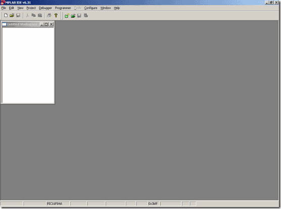
The screen after starting MPLAB
4.3 Designing a project
Preparing the program for loading into microcontroller can boil down to few basic steps:
1. Designing a project
2. Writing the program
3. Converting to zero-one code comprehensible by microcontroller, i.e. compiling.
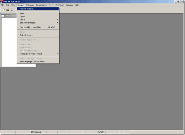
Opening a new project
To create a project, click on the option PROJECT and the click on PROJECT WIZARD, which will open the following window..

Creating a new project
Click on NEXT to continue. Next thing to do is to choose the appropriate microcontroller. In our case, it is PIC16F84A.

Choosing the appropriate microcontroller
Next step is defining the program language to be used. In our case it is Assembler, so we will select that option as shown on the image below.
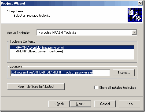
Selecting a language toolsuite
All that is left is to name our project. The name should reflect the purpose and content of the program. Project can be stored in any folder according to your needs. It is a good thing to have that folder remind you of PIC microcontrollers; we named the folder simply PIC in the image below.

Naming the project
Upon naming the project, click on NEXT to open the summary window.

Summary containing the defined parameters
Click on FINISH to create the project. The summary window contains the project parameters.
4.4 Creating a new assembler file
When 'project' part of the job is done, the following screen should appear.
New project opened
Next step is writing the program, which requires new file to be opened. Click on FILE > NEW, opening the text window within the MPLAB working area (new window represents the file program will be written to). Upon opening the new file, it should be saved to folder C:\PIC under a name "Blink.asm", to reflect the nature of the program (example for blinking diodes on microcontroller port B).
New file, "Blink.asm" should now be included into the project. Right-click on the source file in the window "Test.msw". This will open a small window with two available options - choose the first one, "Add Files".
Inserting new Assembler file into project
In a newly opened browse window find our PIC folder and select the file "Blink.asm", as shown on the image below.
Selecting the desired file
The looks of the project window after the file blink.asm has been included is shown in the image below.
4.5 Writing a program
Only after all of the preceding operations have been completed we are able to start writing a program. This sample program is fairly simple and serves to illustrate creation of a project.
You should re-write the program to the newly opened window or just copy/paste it from the disk.
Main window with blink.asm program
When the program is copied to "Blink.asm" window, we can use PROJECT -> BUILD ALL command to translate the program to executable HEX form. The last sentence in the window is the most important one, because it shows whether translation was successful or not. "BUILD SUCCEEDED" is a message stating that translation was successful and that there were no errors.
In case that error does show up, you need to double click on error message in 'Output' window. This will automatically take you to the assembler program, to the line where the error was encountered.
In case that error does show up, you need to double click on error message in 'Output' window. This will automatically take you to the assembler program, to the line where the error was encountered.
4.6 Toolbar icons
The following table contains detailed description of each toolbar icon.
Cut text. This and the following 3 icons are standard for all text processors. As every program code is actually a text file, these options are commonly used.
Copy text. Unlike the previous one, this icon leaves the selected text on screen while storing it into clipboard.
Paste text. When part of the text is copied or cut, it is stored to clipboard, where it can be called upon via this command.
Create a new project. This command is straightforward as it avoids the use of Wizard - just name the project and type the path line to the appropriate folder.
Save Workspace. Workspace saved in this way keeps all the parameter and window settings, so that when it's loaded you get the exact look of the work area it had at the moment of saving. Save your project frequently, especially if you work with multiple windows in simulator and you have them arranged to your liking.
When eventual errors have been spotted during the simulation process, program needs to be repaired. As simulator uses HEX file as its input, program should be translated anew in order to take the changes to the simulator. This icon (Make) translates the project from the start and creates the latest version of the HEX file for the simulator.
Similar to the previous icon, except that the whole project is translated and not just the Assembler file whose code has been changed.
4.7 MPSIM Simulator
Simulator is part of the MPLAB environment which provides a better insight into the workings of a microcontroller. Through a simulator, we can monitor current variable values, register values and status of port pins. Truthfully, simulator does not have the same value in all programs. If a program is simple (like the one given here as an example), simulation is not of great importance because setting port B pins to logic one is not a difficult task. However, simulator can be of great help with more complicated programs which include timers, different conditions where something happens and other similar requirements (especially with mathematical operations). Simulation, as the name indicates "simulates the work of a microcontroller". As microcontroller executes instructions one by one, simulator is conceived - programmer moves through a program step-by-step (line-by-line) and follows what goes on with data within the microcontroller. When writing is completed, it is a good trait for a programmer to first test his program in a simulator, and then run it in a real situation. Unfortunately, as with many other good habits, man tends to avoid this one too, more or less. Reasons for this are partly personality, and partly a lack of good simulators.
Starting the program simulation
Simulator is activated by clicking on DEBUGGER > SELECT TOOL > MPLAB SIM, as shown in the image above. Four new icons appear to the right. They are related to simulator only, and have the following meaning:
Start the program execution at full speed. When started, simulator executes the program until "paused" by the icon below (just as with cassette or CD player).
Stops full-speed program execution. After this icon has been clicked, program execution may be continued step-by-step or at full-speed.
Step Into icon. Step-by-step program execution. Clicking on this icon executes the succeeding program line. It enters the macros and subroutines.
Resets the microcontroller. Clicking on this icon positions the program counter to the beginning of program and simulation may begin.
First thing we need to do, as in a real situation, is to reset a microcontroller with DEBUGGER > RESET command or by clicking on the reset icon. This command results in green marker line positioned at the beginning of the program, and program counter PCL is positioned at zero which can also be seen in Special Functions Registers window.
One of the main simulator features is the ability to view register status within a microcontroller. These registers are also called special function registers, or SFR registers. We can get a window with SFR registers by clicking on VIEW > SPECIAL FUNCTION REGISTERS.
Beside SFR registers, it is useful to have an insight into file registers. Window with file registers can be opened by clicking on VIEW > FILE REGISTERS.
Beside SFR registers, it is useful to have an insight into file registers. Window with file registers can be opened by clicking on VIEW > FILE REGISTERS.
If there are variables in the program, it is good to monitor them, too. Each variable is assigned one window (Watch Windows) by clicking on VIEW > WATCH.
Simulator with open SFR registers and File registers windows
When all the variables and registers of interest are placed on the simulator working area, simulation may begin. Next command can be either Step Into or Step Over, as we may want to go into subroutines or not. Same commands can be issued via keyboard, by clicking F7 or F8.
In the SFR registers window, we can observe how register W receives value 0xFF and delivers it to port B.
By clicking on F7 key again, we don't achieve anything because program has arrived to an "infinite loop". Infinite loop is a term we will meet often. It represents a loop from which a microcontroller cannot get out until interrupt takes place (if it is used in a program), or until a microcontroller is reset.
Macros and subprograms
Introduction
5.1 Macros
5.2 Subprograms
5.3 Macros used in the examples
Introduction
Same or similar sequence of instructions is frequently used during programming. Assembly language is very demanding. Programmer is required to take care of every single detail when writing a program, because just one incorrect instruction or label can bring about wrong results or make the program doesn't work at all. Solution to this problem is to use already tested program parts repeatedly. For this kind of programming logic, macros and subprograms are used.
5.1 Macros
Macro is defined with directive macro containing the name of macro and parameters if needed. In program, definition of macro has to be placed before the instruction line where macro is called upon. When during program execution macro is encountered, it is replaced with an appropriate set of instructions stated in the macro's definition.
macro_name
macro par1, par2,..
set of instructions
set of instructions
endm
The simplest use of macro could be naming a set of repetitive instructions to avoid errors during retyping. As an example, we could use a macro for selecting a bank of SFR registers or for a global permission of interrupts. It is much easier to have a macro BANK1 in a program than having to memorize which status bit defines the mentioned bank. This is illustrated below: banks 0 and 1 are selected by setting or clearing bit 5 (RP0) of status register, while interrupts are enabled by bit 7 of INTCON register. First two macros are used for selecting a bank, while other two enable and disable interrupts.
bank0
macro
; Macro bank0
bcf STATUS, RP0
; Reset RP0 bit = Bank0
endm
; End of macro
bank1
macro
; Macro bank1
bsf STATUS, RP0
; Set RP0 bit = Bank1
endm
; End of macro
enableint
macro
; Interrupts are globally enabled
bsf INTCON, 7
; Set the bit
endm
; End of macro
disableint
macro
; Interrupts are globally disabled
bcf INTCON, 7
; Reset the bit
endm
; End of macro
These macros are to be saved in a special file with extension INC (abbrev. for INCLUDE file). The following image shows the file bank.inc which contains two macros, bank0 and bank1.
Macros Bank0 and Bank1 are given for illustrational purposes more than practical, since directive BANKSEL NameSFR does the same job. Just write BANKSEL TRISB and the bank containing the TRISB register will be selected.
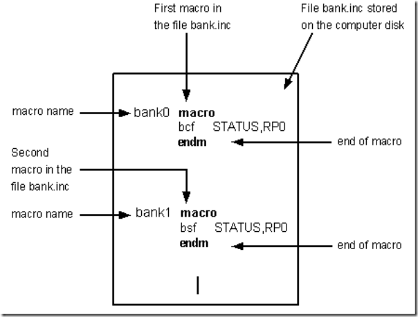
As can be seen above, first four macros do not have parameters. However, parameters can be used if needed. This will be illustrated with the following macros, used for changing direction of pins on ports. Pin is designated as input if the appropriate bit is set (with the position matching the appropriate pin of TRISB register, bank1) , otherwise it's output.
input
macro par1, par2
; Macro input
bank1
; In order to access TRIS registers
bsf par1, par2
; Set the given bit - 1 = input
bank0
; Macro for selecting bank0
endm
; End of macro
output
macro par1, par2
; Macro output
bank1
; In order to access TRIS registers
bcf par1, par2
; Reset the given bit - 0 = output
bank0
; Macro for selecting bank0
endm
; End of macro
Macro with parameters can be called upon in following way:
output TRISB, 7 ; pin RB7 is output
When calling macro first parameter TRISB takes place of the first parameter, par1, in macro's definition. Parameter 7 takes place of parameter par2, thus generating the following code:
output
TRISB, 7
; Macro output
bsf STATUS, RP0
; Set RP0 bit = BANK1
bcf TRISB, 7
; Designate RB7 as output
bcf STATUS, RP0
; Reset RP0 bit = BANK0
endm
; End of macro
Apparently, programs that use macros are much more legible and flexible. Main drawback of macros is the amount of memory used - every time macro name is encountered in the program, the appropriate code from the definition is inserted. This doesn't necessarily have to be a problem, but be warned if you plan to use sizeable macros frequently in your program.
In case that macro uses labels, they have to be defined as local using the directive local. As an example, below is the macro for calling certain function if carry bit in STATUS register is set. If this is not the case, next instruction in order is executed.
callc
macro label
; Macro callc
local
Exit
; Defining local label within macro
bnc Exit
; If C=0 jump to Exit and exit macro
call label
; If C=1 call subprogram at the
; address label outside macro
Exit
; Local label within macro
endm
; End of macro
5.2 Subprograms
Subprogram represents a set of instructions beginning with a label and ending with the instruction return or retlw. Its main advantage over macro is that this set of instructions is placed in only one location of program memory. These will be executed every time instruction call subprogram_name is encountered in program. Upon reaching return instruction, program execution continues at the line succeeding the one subprogram was called from. Definition of subprogram can be located anywhere in the program, regardless of the lines in which it is called.
Label
; subprogram is called with "call Label"
set of instructions
set of instructions
set of instructions
return or retlw
With macros, use of input and output parameters is very significant. With subprograms, it is not possible to define parameters within the subprogram as can be done with macros. Still, subprogram can use predefined variables from the main program as its parameters.
Common course of events would be: defining variables, calling the subprogram that uses them, and then reading the variables which may have been changed by the subprogram.
The following example, addition.asm adds two variables, PAR1 and PAR2, and stores the result to variable RES. As 2-byte variables are in question, lower and higher byte has to be defined for each of these. The program itself is quite simple; it first adds lower bytes of variables PAR1 and PAR2, then it adds higher bytes. If two lower bytes total exceeds 255 (maximum for a byte) carry is added to variable RESH.
Basic difference between macro and subprogram is that the macro stands for its definition code (sparing the programmer from additional typing) and can have its own parameters while subprogram saves memory, but cannot have its own parameters.

5.3 Macros used in the examples
Examples given in chapter 6 frequently use macros ifbit, ifnotbit, digbyte, and pausems, so these will be explained in detail. The most important thing is to comprehend the function of the following macros and the way to use them, without unnecessary bothering with the algorithms itself. All macros are included in the file mikroel84.inc for easier reference.
5.3.1 Jump to label if bit is set
ifbit
macro par1, par2, par3
btfsc par1, par2
goto par3
endm
Macro is called with : ifbit Register, bit, label
5.3.2 Jump to label if bit is cleared
ifnotbit
macro par1, par2, par3
btfss par1, par2
goto par3
endm
Macro is called with : ifnotbit Register, bit, label
Next example shows how to use a macro. Pin 0 on port A is checked and if set, program jumps to label ledoff, otherwise macro ifnotbit executes, directing the program to label ledon.

5.3.3 Extracting ones, tens and hundreds from variable
Typical use for this macro is displaying variables on LCD or 7seg display.
digbyte
macro par0
local Pon0
local Exit1
local Exit2
local Positive
local Negative
clrf Dig1
clrf Dig2
clrf Dig3
Positive
movf par0, w
movwf Digtemp
movlw .100
Pon0
incf Dig1
;computing hundreds digit
subwf Digtemp
btfsc STATUS, C
goto Pon0
decf Dig1, w
addwf Digtemp, f
Exit1
movlw .10
;computing tens digit
incf Dig2, f
subwf Digtemp, f
btfsc STATUS, C
goto Exit1
decf Dig2, f
addwf Digtemp, f
Exit2
movf Digtemp, w
;computing ones digit
movwf Dig3
endm
Macro is called with :
movlw .156
; w = 156
movwf RES
; RES = w
digbyte RES
; now Dec1<-1, Dec2<-5, Dec3<-6
The following example shows how to use macro digbyte in program. At the beginning, we have to define variables for storing the result, Dig1, Dig2, Dig3, as well as auxiliary variable Digtemp.

5.3.4 Generating pause in miliseconds (1~65535ms)
Purpose of this macro is to provide exact time delays in program.
pausems
macro par1
local
Loop1
local
dechi
local
Delay1ms
local
Loop2
local
End
movlw high par1
; Higher byte of parameter 1 goes to HIcnt
movwf HIcnt
movlw low par1
; Lower byte of parameter 1 goes to LOcnt
movwf LOcnt
Loop1
movf LOcnt, f
; Decrease HIcnt and LOcnt necessary
btfsc STATUS, Z
; number of times and call subprogram Delay1ms
goto dechi
call Delay1ms
decf LOcnt, f
goto Loop1
dechi
movf HIcnt, f
btfsc STATUS, Z
goto End
call Delay1ms
decf HIcnt, f
decf LOcnt, f
goto Loop1
Delay1ms:
; Delay1ms produces a one milisecond delay
movlw .100
; 100*10us=1ms
movwf LOOPcnt
; LOOPcnt<-100
Loop2:
nop
nop
nop
nop
nop
nop
nop
decfsz LOOPcnt, f
goto Loop2
; Time period necessary to execute loop Loop2
return
; equals 10us
End
endm
This macro is written for an 4MHz oscillator. For instance, with 8MHz oscillator, pause will be halved. It has very wide range of applications, from simple code such as blinking diodes to highly complicated programs that demand accurate timing. Following example demonstrates use of macro pausems in a program. At the beginning of the program we have to define auxiliary variables HIcnt, LOcnt, and LOPcnt.

CHAPTER 6
Examples for subsystems within microcontroller
6.1 Writing to and reading from EEPROM
6.2 Processing interrupt caused by changes on pins RB4-RB7
6.3 Processing interrupt caused by change on pin RB0
6.4 Processing interrupt caused by overflow on timer TMR0
6.5 Processing interrupt caused by overflow on TMR0 connected to external input (TOCKI)
6.2 Processing interrupt caused by changes on pins RB4-RB7
6.3 Processing interrupt caused by change on pin RB0
6.4 Processing interrupt caused by overflow on timer TMR0
6.5 Processing interrupt caused by overflow on TMR0 connected to external input (TOCKI)
Every microcontroller comprises a number of subsystems allowing for flexibility and wide range of applications. These include internal EEPROM memory, AD converters, serial or other form of communication, timers, interrupts, etc. Two most commonly utilized elements are interrupts and timers. One of these or several in combination can create a basis for useful and practical programs.
Program "eeprom.asm" uses EEPROM memory for storing certain microcontroller parameters. Transfer of data between RAM and EEPROM has two steps - calling macros eewrite and eeread. Macro eewrite writes certain variable to a given address, while eeread reads the given address of EEPROM and stores the value to a variable.
Macro eewrite writes the address to EEADR register and the variable to EEDATA register. It then calls the subprogram which executes the standard procedure for initialization of writing data (setting WREN bit in EECON1 register and writing control bytes 0x55 and 0xAA to EECON2).
For data to be actually stored in EEPROM, 10ms delay is necessary. This is achieved by using macro pausems. In case that this pause is unacceptable for any reason, problem can be solved by using an interrupt for signaling that data is written to EEPROM.
eewrite
macro addr, var
macro addr, var
addr
Destination address. With PIC16F84, there are 68 bytes
Destination address. With PIC16F84, there are 68 bytes
of EEPROM for a total address range of 0x00 - 0x44.
var
Name of the variable to be stored to EPROM
Name of the variable to be stored to EPROM
eeread
macro addr, var
macro addr, var
addr
Destination address. With PIC16F84, there are 68 bytes
Destination address. With PIC16F84, there are 68 bytes
of EEPROM for a total address range of 0x00 - 0x44.
var
Name of the variable into which data read from EPROM will be stored.
Name of the variable into which data read from EPROM will be stored.
Example: Variable volume, which is set via buttons RA0 and RA1, will be stored to the address 0 of EEPROM. After reboot, when the program is started, it first loads the last known value of variable volume from EEPROM.
Program "intportb.asm" illustrates how interrupt can be employed for indicating changes on pins RB4-RB7. Upon pushing any of the buttons, program enters the interrupt routine and determines which pin caused an interrupt. This program could be utilized in systems with battery power supply, where power consumption plays an important role. It is useful to set microcontroller to low consumption mode with a sleep instruction. Microcontroller is practically on stand-by, saving energy until the occurrence of interrupt.
Example of processing interrupt caused by changes on pins RB4-RB7
Example "intrb0.asm" demonstrates use of interrupt RB0/INT. Upon falling edge of the impulse coming to RB0/INT pin, program jumps to subprogram for processing interrupt. This routine then performs a certain operation, in our case it blinks the LED diode on PORTB, 7.
Example of processing interrupt caused by changes on pin RB0
Program "inttmr0.asm" illustrates how interrupt TMR0 can be employed for generating specific periods of time. Diodes on port B are switched on and off alternately every second. Interrupt is generated every 5.088ms; in interrupt routine variable cnt is incremented to the cap of 196, thus generating approx. 1 second pause (5.088ms*196 is actually 0.99248s). Pay attention to initialization of OPTION register which enables this mode of work for timer TMR0.
Example of processing interrupt caused by overflow on timer TMR0
Counter TMR0 increments upon signal change on pin RA4/TOCKI. Prescaler is set to 4, meaning that TMR0 will be incremented on every fourth impulse. Pay attention to initialization of OPTION register which enables this mode of work for timer TMR0 (this mode is common for devices such as counters).
Example of processing interrupt caused by overflow on timer TMR0 connected to TOCKI
CHAPTER 7
Examples
Introduction
7.1 Supplying the microcontroller
7.2 LED diodes
7.3 Push buttons
7.4 Optocoupler
7.4.1 Optocouper on input line
7.4.2 Optocoupler on output line
7.5 Relay
7.6 Generating sound
7.7 Shift registers
7.7.1 Input shift register
7.7.2 Output shift register
7.8 7-seg display (multiplexing)
7.9 LCD display
7.10 Software SCI communication
Introduction
Examples given in this chapter will show you how to connect the PIC microcontroller with other peripheral components or devices when developing your own microcontroller system. Each example contains detailed description of hardware with electrical outline and comments on the program. All programs can be taken directly from the 'MikroElektronika' Internet presentation.
7.1 Supplying the microcontroller
Generally speaking, the correct voltage supply is of utmost importance for the proper functioning of the microcontroller system. It can easily be compared to a man breathing in the air. It is more likely that a man who is breathing in fresh air will live longer than a man who's living in a polluted environment.
For a proper function of any microcontroller, it is necessary to provide a stable source of supply, a sure reset when you turn it on and an oscillator. According to technical specifications by the manufacturer of PIC microcontroller, supply voltage should move between 2.0V to 6.0V in all versions. The simplest solution to the source of supply is using the voltage stabilizer LM7805 which gives stable +5V on its output. One such source is shown in the picture below.

In order to function properly, or in order to have stable 5V at the output (pin 3), input voltage on pin 1 of LM7805 should be between 7V through 24V. Depending on current consumption of device we will use the appropriate type of voltage stabilizer LM7805. There are several versions of LM7805. For current consumption of up to 1A we should use the version in TO-220 case with the capability of additional cooling. If the total consumption is 50mA, we can use 78L05 (stabilizer version in small TO - 92 packaging for current of up to 100mA).
7.2 LED diodes
LEDs are surely one of the most commonly used elements in electronics. LED is an abbreviation for 'Light Emitting Diode'. When choosing a LED, several parameters should be looked at: diameter, which is usually 3 or 5 mm (millimeters), working current which is usually about 10mA (It can be as low as 2mA for LEDs with high efficiency - high light output), and color of course, which can be red or green though there are also orange, blue, yellow....
LEDs must be connected around the correct way, in order to emit light and the current-limiting resistor must be the correct value so that the LED is not damaged or burn out (overheated). The positive of the supply is taken to the anode, and the cathode goes to the negative or ground of the project (circuit). In order to identify each lead, the cathode is the shorter lead and the LED "bulb" usually has a cut or "flat" on the cathode side. Diodes will emit light only if current is flowing from anode to cathode. Otherwise, its PN junction is reverse biased and current won't flow. In order to connect a LED correctly, a resistor must be added in series that to limit the amount of current through the diode, so that it does not burn out. The value of the resistor is determined by the amount of current you want to flow through the LED. Maximum current flow trough LED was defined by manufacturer.
LEDs must be connected around the correct way, in order to emit light and the current-limiting resistor must be the correct value so that the LED is not damaged or burn out (overheated). The positive of the supply is taken to the anode, and the cathode goes to the negative or ground of the project (circuit). In order to identify each lead, the cathode is the shorter lead and the LED "bulb" usually has a cut or "flat" on the cathode side. Diodes will emit light only if current is flowing from anode to cathode. Otherwise, its PN junction is reverse biased and current won't flow. In order to connect a LED correctly, a resistor must be added in series that to limit the amount of current through the diode, so that it does not burn out. The value of the resistor is determined by the amount of current you want to flow through the LED. Maximum current flow trough LED was defined by manufacturer.
To determine the value of the dropper-resistor, we need to know the value of the supply voltage. From this we subtract the characteristic voltage drop of a LED. This value will range from 1.2v to 1.6v depending on the color of the LED. The answer is the value of Ur. Using this value and the current we want to flow through the LED (0.002A to 0.01A) we can work out the value of the resistor from the formula R=Ur/I.
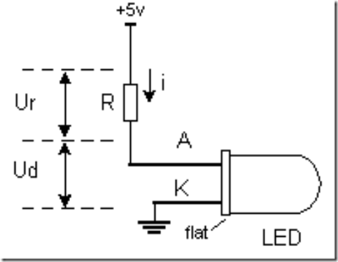

LEDs are connected to a microcontroller in two ways. One is to switch them on with logic zero, and other to switch them on with logic one. The first is called NEGATIVE logic and the other is called POSITIVE logic. The next diagram shows how to connect POSITIVE logic. Since POSITIVE logic provides a voltage of +5V to the diode and dropper resistor, it will emit light each time a pin of port B is provided with a logic 1. The other way is to connect all anodes to +5V and to deliver logical zero to cathodes.
Connecting LED diodes to PORTB microcontroller
The following example initializes port B as output and alternately switches on and off LED diodes every 0.5sec. For pause we used macro pausems, which is defined in the file mikroel84.inc.
7.3 Push buttons
Buttons are mechanical devices used to execute a break or make connection between two points. They come in different sizes and with different purposes. Buttons that are used here are also called "dip-buttons". They are soldered directly onto a printed board and are common in electronics. They have four pins (two for each contact) which give them mechanical stability.
Example of connecting buttons to microcontroller pins
Button function is simple. When we push a button, two contacts are joined together and connection is made. Still, it isn't all that simple. The problem lies in the nature of voltage as an electrical dimension, and in the imperfection of mechanical contacts. That is to say, before contact is made or cut off, there is a short time period when vibration (oscillation) can occur as a result of unevenness of mechanical contacts, or as a result of the different speed in pushing a button (this depends on person who pushes the button). The term given to this phenomena is called SWITCH (CONTACT) DEBOUNCE. If this is overlooked when program is written, an error can occur, or the program can produce more than one output pulse for a single button push. In order to avoid this, we can introduce a small delay when we detect the closing of a contact. This will ensure that the push of a button is interpreted as a single pulse. The debounce delay is produced in software and the length of the delay depends on the button, and the purpose of the button. The problem can be partially solved by adding a capacitor across the button, but a well-designed program is a much-better answer. The program can be adjusted until false detection is completely eliminated. Image below shows what actually happens when button is pushed.
As buttons are very common element in electronics, it would be smart to have a macro for detecting the button is pushed. Macro will be called button. Button has several parameters that deserve additional explanation.
button macro port, pin, hilo, label
Port is a microcontroller's port to which a button is connected. In case of a PIC16F84 microcontroller, it can be PORTA or PORTB.
Pin is port's pin to which the button is connected.
HiLo can be '0' or '1' which represents the state when the button is pushed.
Label is a destination address for jump to a service subprogram which will handle the event (button pushed).
Example 1:
button PORTA, 3, 1, Button1
Button T1 is connected to pin RA3 and to the mass across a pull-down resistor, so it generates logical one upon push. When the button is released, program jumps to the label Button1.
Example 2:
button PORTA, 2, 0, Button2
Button T1 is connected to pin RA1 and to the mass across a pull-up resistor, so it generates logical zero upon push. When the button is released, program jumps to the label Button2.
The following example illustrates use of macro button in a program. Buttons are connected to the supply across pull-up resistors and connect to the mass when pushed. Variable cnt is displayed on port B LEDs; cnt is incremented by pushing the button RA0, and is decremented by pushing the button RA1.
It is important to note that this kind of debouncing has certain drawbacks, mainly concerning the idle periods of microcontroller. Namely, microcontroller is in the state of waiting from the moment the button is pushed until it is released, which can be a very long time period in certain applications. if you want the program to be attending to a number of things at the same time, different approach should be used from the start. Solution is to use the interrupt routine for each push of a button, which will occur periodically with pause adequate to compensate for repeated pushes of button.
The idea is simple. Every 10ms, button state will be checked upon and compared to the previous input state. This comparison can detect rising or falling edge of the signal. In case that states are same, there were apparently no changes. In case of change from 0 to a 1, rising edge occurred. If succeeding 3 or 4 checks yield the same result (logical one), we can be positive that the button is pushed.
7.4 Optocouplers
Optocouplers were discovered right aer photo-transistors (like any other transistor, except it is stimulated by light), by combining a LED and photo-transistor in the same case. The purpose of an optocoupler is to separate two parts of a circuit.
This is done for a number of reasons:
- Interference. Typical examples are industrial units with lots of interferences which affect signals in the wires. If these interferences affected the function of control section, errors would occur and the unit would stop working.
- Simultaneous separation and intensification of a signal. Typical examples are relays which require higher current than microcontroller pin can provide. Usually, optocoupler is used for separating microcontroller supply and relay supply.
- In case of a breakdown, optocoupled part of device stays safe in its casing, reducing the repair costs.
Optocouplers can be used as either input or output devices. They can have additional functions such as intensification of a signal or Schmitt triggering (the output of a Schmitt trigger is either 0 or 1 - it changes slow rising and falling waveforms into definite low or high values). Optocouplers come as a single unit or in groups of two or more in one casing. Each optocoupler needs two supplies in order to function. They can be used with one supply, but the voltage isolation feature, which is their primary purpose, is lost.
7.4.1 Optocoupler on an input line
The way it works is simple: when a signal arrives, the LED within the optocoupler is turned on, and it illuminates the base of a photo-transistor within the same case. When the transistor is activated, the voltage between collector and emitter falls to 0.7V or less and the microcontroller sees this as a logic zero on its RA4 pin.
The example below is a simplified model of a counter, element commonly utilized in industry (it is used for counting products on a production line, determining motor speed, counting the number of revolutions of an axis, etc). We will have sensor set off the LED every time axis makes a full revolution. LED in turn will 'send' a signal by means of photo-transistor to a microcontroller input RA4 (TOCKI). As prescaler is set to 1:2 in this example, every second signal will increment TMR0. Current status of the counter is displayed on PORTB LEDs.
Example of optocoupler on an input line
7.4.2 Optocoupler on an output line
An Optocoupler can be also used to separate the output signals. If optocoupler LED is connected to microcontroller pin, logical zero on pin will activate optocoupler LED, thus activating the transistor. This will consequently switch on LED in the part of device working on 12V. Layout of this connection is shown below.
Example of optocoupler on output line
The program for this example is simple. By delivering a logical one to the third pin of port A, the transistor will be activated in the optocoupler, switching on the LED in the part of device working on 12V.
7.5 Relay
The relay is an electromechanical device, which transforms an electrical signal into mechanical movement. It consists of a coil of insulated wire on a metal core, and a metal armature with one or more contacts. When a supply voltage was delivered to the coil, current would flow and a magnetic field would be produced that moves the armature to close one set of contacts and/or open another set. When power is removed from the relay, the magnetic flux in the coil collapses and produces a fairly high voltage in the opposite direction. This voltage can damage the driver transistor and thus a reverse-biased diode is connected across the coil to "short-out" the spike when it occurs.
Connecting a relay to the microcontroller via transistor
Since microcontroller cannot provide sufficient supply for a relay coil (approx. 100+mA is required; microcontroller pin can provide up to 25mA), a transistor is used for adjustment purposes, its collector circuit containing the relay coil. When a logical one is delivered to transistor base, transistor activates the relay, which then, using its contacts, connects other elements in the circuit. Purpose of the resistor at the transistor base is to keep a logical zero on base to prevent the relay from activating by mistake. This ensures that only a clean logical one on RA3 activates the relay.
Connecting the optocoupler and relay to a microcontroller
A relay can also be activated via an optocoupler which at the same time amplifies the current related to the output of the microcontroller and provides a high degree of isolation. High current optocouplers usually contain a 'Darlington' output transistor to provide high output current.
Connecting via an optocoupler is recommended especially for microcontroller applications, where relays are used fro starting high power load, such as motors or heaters, whose voltage instability can put the microcontroller at risk. In our example, when LED is activated on some of the output port pins, the relay is started. Below is the program needed to activate the relay, and includes some of the already discussed macros.
In microcontroller systems, beeper is used for indicating certain occurrences, such as push of a button or an error. To have the beeper started, it needs to be delivered a string in binary code - in this way, you can create sounds according to your needs. Connecting the beeper is fairly simple: one pin is connected to the mass, and the other to the microcontroller pin through a capacitor, as shown on the following image.

As with a button, you can employ a macro that will deliver a BEEP ROUTINE into a program when needed. Macro BEEP has two arguments:
BEEP macro freq , duration:
freq: frequency of the sound. The higher number produces higher frequency
duration: sound duration. Higher the number, longer the sound.
Example 1: BEEP 0xFF, 0x02
The output has the highest frequency and duration at 2 cycles per 65.3mS which gives 130.6 mS
Example2: BEEP 0x90, 0x05
The output has a frequency of 0x90 and duration of 5 cycles per 65.3mS. It is best to determine these macro parameters through experimentation and select the sound that best suits the application.
The following is the BEEP Macro listing:

The following example shows the use of a macro in a program. The program produces two melodies which are obtained by pressing T1 or T2. Some of the previously discussed macros are included in the program.

7.7 Shift registers
There are two types of shift registers: input and output. Input shift registers receive data in parallel, through 8 lines and then send it serially through two lines to a microcontroller. Output shift registers work in the opposite direction; they receive serial data and on a "latch" line signal, they turn it into parallel data. Shift registers are generally used to expand the number of input-output lines of a microcontroller. They are not so much in use any more though, because most modern microcontrollers have a large number of pins. However, their use with microcontrollers such as PIC16F84 is very important.
7.7.1 Input shift register 74HC597
Input shift registers transform parallel data into serial data and transfers it to a microcontroller. Their working is quite simple. There are four lines for the transfer of data: Clock, Latch, Load and Data. Data is first read from the input pins by an internal register through a 'latch' signal. Then, with a 'load' signal, data is transferred from the input latch register to the shift register, and from there it is serially transferred to a microcontroller via 'data' and 'clock' lines.
An outline of the connection of the shift register 74HC597 to a micro, is shown below.
In order to simplify the main program, a macro can be used for the input shift register. Macro HC597 has two parameters:
HC597 macro Var, Var1
Var variable where data from shift register input pins is transferred
Var1 loop counter
Example: HC597 data, counter
Data from the input pins of the shift register is stored in data variable. Timer/counter variable is used as a loop counter.
Macro listing:
HC597 macro Var, Var1
Var variable where data from shift register input pins is transferred
Var1 loop counter
Example: HC597 data, counter
Data from the input pins of the shift register is stored in data variable. Timer/counter variable is used as a loop counter.
Macro listing:
Example of how to use the HC597 macro is given in the following program. Program receives data from a parallel input of the shift register and moves it serially into the RX variable of the microcontroller. LEDs connected to port B will indicate the result of the data input.
7.7.2 Output shift register
Output shift registers transform serial data into parallel data. On every rising edge of the clock, the shift register reads the value from data line, stores it in temporary register, and then repeats this cycle 8 times. On a signal from 'latch' line, data is copied from the shift register to input register, thus data is transformed from serial into parallel data.
An outline of the 74HC595 shift register connections is shown on the diagram below:
Macro used in this example can be found in hc595.inc file, and is called HC595.
Macro HC595 has two parameters:
HC595 macro Var, Var1
Var variable whose contents is transferred to outputs of shift register.
Var1 loop counter
Example: HC595 Data, counter
The data we want to transfer is stored in data variable, and counter variable is used as a loop counter.
Macro HC595 has two parameters:
HC595 macro Var, Var1
Var variable whose contents is transferred to outputs of shift register.
Var1 loop counter
Example: HC595 Data, counter
The data we want to transfer is stored in data variable, and counter variable is used as a loop counter.
An example of how to use the HC595 macro is given in the following program. Data from variable TX is serially transferred to shift register. LEDs connected to the parallel output of the shift register will indicate the state of the lines. In this example value 0xCB (1100 1011) is sent so that the seventh, sixth, third, first, and zero LEDs are illuminated.
The segments in a 7-segment display are arranged to form a single digit from 0 to F as shown in the animation:

We can display a multi-digit number by connecting additional displays. Even though LCD displays are more comfortable to work with, 7-segment displays are still standard in the industry. This is due to their temperature robustness, visibility and wide viewing angle. Segments are marked with non-capital letters: a, b, c, d, e, f, g and dp, where dp is the decimal point. The 8 LEDs inside each display can be arranged with a common cathode or common anode. With a common cathode display, the common cathode must be connected to the 0V rail and the LEDs are turned on with a logic one. Common anode displays must have the common anode connected to the +5V rail. The segments are turned on with a logic zero. The size of a display is measured in millimeters, the height of the digit itself (not the housing, but the digit!). Displays are available with a digit height of 7,10, 13.5, 20, or 25 millimeters. They come in different colors, including: red, orange, and green.
The simplest way to drive a display is via a display driver. These are available for up to 4 displays. Alternatively displays can be driven by a microcontroller and if more than one display is required, the method of driving them is called "multiplexing."
The main difference between the two methods is the number of "drive lines." A special driver may need only a single "clock" line and the driver chip will access all the segments and increment the display. If a single display is to be driven from a microcontroller, 7 lines will be needed plus one for the decimal point. For each additional display, only one extra line is needed. To produce a 4, 5 or 6 digit display, all the 7-segment displays are connected in parallel. The common line (the common-cathode line) is taken out separately and this line is taken low for a short period of time to turn on the display. Each display is turned on at a rate above 100 times per second, and it will appear that all the displays are turned on at the same time. As each display is turned on, the appropriate information must be delivered to it so that it will give the correct reading. Up to 6 displays can be accessed like this without the brightness of each display being affected. Each display is turned on very hard for one-sixth the time and the POV (persistence of vision) of our eye thinks the display is turned on the whole time. Therefore, the program has to ensure the proper timing, else the unpleasant blinking of display will occur.
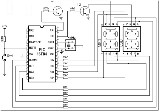
Connecting a microcontroller to 7-segment displays in multiplex mode
Program "7seg.asm" displays decimal value of a number stored in variable D.
Example:
movlw .21
movlw D
; number 21 will be printed on 7seg display
Displaying digits is carried out in multiplex mode which means that the microcontroller alternately prints ones digit and tens digit. TMR0 interrupt serves for generating a time period, so that the program enters the interrupt routine every 5ms and performs multiplexing. In the interrupt routine, first step is deciding which segment should be turned on. In case that the tens digit was previously on, it should be turned off, set the mask for printing the ones digit on 7seg display which lasts 5ms, i.e. until the next interrupt.
For extracting the ones digit and the tens digit, macro digbyte is used. It stores the hundreds digit, the tens digit, and the ones digit into variables Dig1, Dig2, and Dig3. In our case, upon macro execution, Dig1 will equal 0, Dig2 will equal 2, and Dig3 will equal 1.
Realization of the macro is given in the following listing:

The following example shows the use of the macro in a program. Program prints a specified 2-digit number on a 7seg display in multiplex mode.
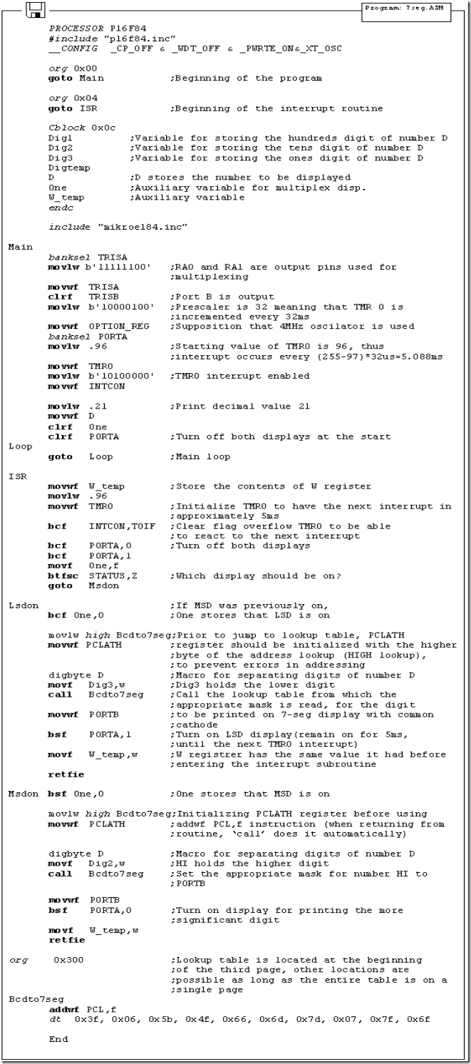
More microcontroller devices are using 'smart LCD' displays to output visual information. The following discussion covers the connection of a Hitachi LCD display to a PIC microcontroller. LCD displays designed around Hitachi's LCD HD44780 module, are inexpensive, easy to use, and it is even possible to produce a readout using the 8 x 80 pixels of the display. Hitachi LCD displays have a standard ASCII set of characters plus Japanese, Greek and mathematical symbols.

A 16x2 line Hitachi HD44780 display
For a 8-bit data bus, the display requires a +5V supply plus 11 I/O lines. For a 4-bit data bus it only requires the supply lines plus seven extra lines. When the LCD display is not enabled, data lines are tri-state which means they are in a state of high impendance (as though they are disconnected) and this means they do not interfere with the operation of the microcontroller when the display is not being addressed.
The LCD also requires 3 "control" lines from the microcontroller.
Enable (E)
This line allows access to the display through R/W and RS lines. When this line is low, the LCD is disabled and ignores signals from R/W and RS. When (E) line is high, the LCD checks the state of the two control lines and responds accordingly.
Read/Write (R/W)
This line determines the direction of data between the LCD and microcontroller. When it is low, data is written to the LCD. When it is high, data is read from the LCD.
Register select (RS)
With the help of this line, the LCD interprets the type of data on data lines. When it is low, an instruction is being written to the LCD. When it is high, a character is being written to the LCD.
Logic status on control lines:
E 0 Access to LCD disabled
1 Access to LCD enabled
R/W 0 Writing data to LCD
1 Reading data from LCD
RS 0 Instruction
1 Character
Writing data to the LCD is done in several steps:
Set R/W bit to low
Set RS bit to logic 0 or 1 (instruction or character)
Set data to data lines (if it is writing)
Set E line to high
Set E line to low
Read data from data lines (if it is reading)
Reading data from the LCD is done in the same way, but control line R/W has to be high. When we send a high to the LCD, it will reset and wait for instructions. Typical instructions sent to LCD display after a reset are: turning on a display, turning on a cursor and writing characters from left to right. When the LCD is initialized, it is ready to continue receiving data or instructions. If it receives a character, it will write it on the display and move the cursor one space to the right. The Cursor marks the next location where a character will be written. When we want to write a string of characters, first we need to set up the starting address, and then send one character at a time. Characters that can be shown on the display are stored in data display (DD) RAM. The size of DDRAM is 80 bytes.
The LCD display also possesses 64 bytes of Character-Generator (CG) RAM. This memory is used for characters defined by the user. Data in CG RAM is represented as an 8-bit character bit-map. Each character takes up 8 bytes of CG RAM, so the total number of characters, which the user can define is eight. In order to read in the character bit-map to the LCD display, we must first set the CG RAM address to starting point (usually 0), and then write data to the display. The definition of a 'special' character is given in the picture.

Before we access DD RAM after defining a special character, the program must set the DD RAM address. Writing and reading data from any LCD memory is done from the last address which was set up using set-address instruction. Once the address of DD RAM is set, a new written character will be displayed at the appropriate place on the screen. Until now we discussed the operation of writing and reading to an LCD as if it were an ordinary memory. But this is not so. The LCD controller needs 40 to 120 microseconds (uS) for writing and reading. Other operations can take up to 5 mS. During that time, the microcontroller can not access the LCD, so a program needs to know when the LCD is busy. We can solve this in two ways.

One way is to check the BUSY bit found on data line D7. This is not the best method because LCD's can get stuck, and program will then stay forever in a loop checking the BUSY bit. The other way is to introduce a delay in the program. The delay has to be long enough for the LCD to finish the operation in process. Instructions for writing to and reading from an LCD memory are shown in the previous table.
At the beginning we mentioned that we needed 11 I/O lines to communicate with an LCD. However, we can communicate with an LCD through a 4-bit data bus. Thus we can reduce the total number of communication lines to seven. The wiring for connection via a 4-bit data bus is shown in the diagram below. In this example we use an LCD display with 2x16 characters, labeled LM16X212 by Japanese maker SHARP. The message 'character' is written in the first row: and two special characters '~' and '}' are displayed. In the second row we have produced the word 'mikroElektronika'.

Connecting an LCD display to a microcontroller
File lcd.inc contains a group of macros for use when working with LCD displays.

Using the macro for LCD support
lcdinit
Macro used to initialize port connected to LCD. LCD is configured to work in 4-bit mode.
Example:
lcdinit
lcdtext
lcdtext prints the text of up to 16 characters, which is specified as a macro parameter. First parameter selects the line in which to start printing. If select is zero, text is printed from the current cursor position.
Example:
lcdtext 1, "mikroelektronika"
lcdtext 1, "Temperature1" ;Print the text starting from line 1, character 1
lcdtext 2, "temp=" ;Print the text starting from line 2, character 1
lcdtext 0, " C" ;Print C in the rest of the line 2
lcdcmd
Sends command instructions
LCDCLR
= b'00000001'
;Clear display, cursor home
LCDCH
= b'00000010'
;Cursor home
LCDCL
= b'00000100'
;Move the cursor to the left
LCDCR
= b'00000110'
;Move the cursor to the right
LCDSL
= b'00011000'
;Move the content of display to the left
LCDSR
= b'00011100'
;Move the content of display to the right
LCDL1
= b'10000000'
;Select line 1
LCDL2
= b'11000000'
;Select line 2
Example:
lcdcmd LCDCH
lcdbyte
Prints one byte variable and omits leading zeros
Example:
lcdbyte Temperature
When working with a microcontroller the numbers are presented in a binary form. As such, they cannot be displayed on a display. That's why it is necessary to change the numbers from a binary system into a decimal system so they can be easily understood. For printing the variables lcdbyte and lcdword we have used the macros digbyte and digword which convert the numbers from binary system into a decimal system and print the result on LCD. Main program has the purpose of demonstrating use of LCD display. At the start it's necessary to declare variables LCDbuf, LCDtemp, Digtemp, Dig1, Dig2, and Dig3 used by the macros for LCD support. It is also necessary to state the port of microcontroller that LCD is connected to. Program initializes the LCD and demonstrates printing text and 8-bit variable temp.

Instruction Set
Introduction
Instruction set in PIC16Cxx microcontroller family
Data Transfer
Arithmetic and logic
Bit operations
Directing the program flow
Instruction execution period
Word list
Instruction list
Instruction set in PIC16Cxx microcontroller family
Data Transfer
Arithmetic and logic
Bit operations
Directing the program flow
Instruction execution period
Word list
Instruction list
We have already mentioned that microcontroller is not like any other integrated circuit. When they come out of production most integrated circuits are ready to be built into devices which is not the case with microcontrollers. In order to "make" microcontroller perform a task, we have to tell it exactly what to do, or in other words we must write the program microcontroller will execute. We will describe in this chapter instructions which make up the assembler, or lower-level program language for PIC microcontrollers.
Complete set which includes 35 instructions is given in the following table. A reason for such a small number of instructions lies primarily in the fact that we are talking about a RISC microcontroller whose instructions are well optimized considering the speed of work, architectural simplicity and code compactness. The only drawback is that programmer is expected to master "uncomfortable" technique of using a reduced set of 35 instructions.
Transfer of data in a microcontroller is done between work (W) register and an 'f' register that represents any location in internal RAM (regardless whether those are special or general purpose registers).
First three instructions (look at the following table) provide for a constant being written in W register (MOVLW is short for MOVe Literal to W), and for data to be copied from W register onto RAM and data from RAM to be copied onto W register (or on the same RAM location, at which point only the status of Z flag changes). Instruction CLRF writes constant 0 in 'f ' register, and CLRW writes constant 0 in register W. SWAPF instruction exchanges places of the 4-bit nibbles field inside a register.
First three instructions (look at the following table) provide for a constant being written in W register (MOVLW is short for MOVe Literal to W), and for data to be copied from W register onto RAM and data from RAM to be copied onto W register (or on the same RAM location, at which point only the status of Z flag changes). Instruction CLRF writes constant 0 in 'f ' register, and CLRW writes constant 0 in register W. SWAPF instruction exchanges places of the 4-bit nibbles field inside a register.
Of all arithmetic operations, PIC like most microcontrollers supports only subtraction and addition. Flags C, DC and Z are set depending on a result of addition or subtraction, but with one exception: since subtraction is performed like addition of a negative value, C flag is inverse following a subtraction. In other words, it is set if operation is possible, and reset if larger number was subtracted from a smaller one.
Logic unit of PIC has capability of performing operations AND, OR, EX-OR, complementing (COMF) and rotation (RLF and RRF).
Instructions which rotate the register contents move bits inside a register through flag C by one space to the left (toward bit 7), or to the right (toward bit 0). Bit which "comes out" of a register is written in flag C, and value of C flag is written in a bit on the "opposite side" of the register.
Instructions BCF and BSF do setting or cleaning of one bit anywhere in the memory. Even though this seems like a simple operation, it is executed so that CPU first reads the whole byte, changes one bit in it and then writes in the entire byte at the same place.
Instructions GOTO, CALL and RETURN are executed the same way as on all other microcontrollers, only stack is independent of internal RAM and limited to eight levels.
'RETLW k' instruction is identical with RETURN instruction, except that before coming back from a subprogram a constant defined by instruction operand is written in W register. This instruction enables us to design easily the Look-up tables (lists). Mostly we use them by determining data position on our table adding it to the address at which the table begins, and then we read data from that location (which is usually found in program memory).
Table can be formed as a subprogram which consists of a series of 'RETLW k' instructions, where 'k' constants are members of the table.
We write the position of a member of our table in W register, and using CALL instruction we call a subprogram which creates the table. First subprogram line ADDWF PCL, f adds the position of a W register member to the starting address of our table, found in PCL register, and so we get the real data address in program memory. When returning from a subprogram we will have in W register the contents of an addressed table member. In a previous example, constant 'k2' will be in W register following a return from a subprogram.
RETFIE (RETurn From Interrupt - Interrupt Enable) is a return from interrupt routine and differs from a RETURN only in that it automatically sets GIE (Global Interrupt Enable) bit. Upon an interrupt, this bit is automatically cleared. As interrupt begins, only the value of program counter is put at the top of a stack. No automatic storing of register values and status is provided.
Conditional jumps are synthesized into two instructions: BTFSC and BTFSS. Depending on a bit status in 'f' register that is being tested, instructions skip or don't skip over the next program instruction.
All instructions are executed in one cycle except for conditional branch instructions if condition was true, or if the contents of program counter was changed by some instruction. In that case, execution requires two instruction cycles, and the second cycle is executed as NOP (No Operation). Four oscillator clocks make up one instruction cycle. If we are using an oscillator with 4MHz frequency, the normal time for executing an instruction is 1 µs, and in case of conditional branching, execution period is 2 µs.
f any memory location in a microcontroller
W work register
b bit position in 'f' register
d destination bit
label group of eight characters which marks the beginning of a part of the program
TOS top of stack
[] option
<> bit position inside register
W work register
b bit position in 'f' register
d destination bit
label group of eight characters which marks the beginning of a part of the program
TOS top of stack
[] option
<> bit position inside register
*1 If I/O port is source operand, status on microcontroller pins is read
*2 If this instruction is executed on TMR register and if d=1, prescaler assigned to that timer will automatically be cleared
*3 If PC was modified, or test result =1, instruction was executed in two cycles.
*2 If this instruction is executed on TMR register and if d=1, prescaler assigned to that timer will automatically be cleared
*3 If PC was modified, or test result =1, instruction was executed in two cycles.
Appendix contains all instructions presented separately with examples for their use. Syntax, description and its effects on status bits are given for each instruction.
Numerical Systems
Introduction
B.1 Decimal numerical system
B.2 Binary numerical system
B.3 Hexadecimal numerical system
Introduction
It was always difficult for people to accept the fact that some things differ from them or their way of thinking. That is probably one of the reasons why numerical systems which differ from a decimal are still hard to understand. Still, whether we want it or not, reality is different. Decimal numerical system that people use in everyday life is so far behind the binary system used by millions of computers around the world.
Each numerical system are based on some basis. With a decimal numerical system, that basis is 10, with binary 2, and with a hexadecimal system 16. The value of each decimal is determined by its position in relation to the whole number represented in the given numerical system. The sum of values of each decimal gives the value of the whole number. Binary and hexadecimal numerical systems are especially interesting for the subject of this book. Beside these, we will also discuss a decimal system, in order to compare it with the other two. Even though a decimal numerical system is a subject we are well acquainted with, we will discuss it here because of its relatedness to other numerical systems.
B.1 Decimal numerical system
Decimal numerical system is defined by its basis 10 and decimal space that is counted from right to left, and consists of numbers 0,1, 2, 3, 4, 5, 6, 7, 8, 9. That means that the end right digit of the total sum is multiplied by 1, next one by 10, next by 100, etc.
Example:
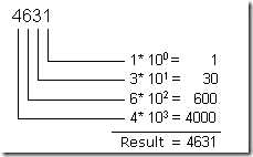
Operations of addition, subtraction, division, and multiplication in a decimal numerical system are used in a way that is already known to us, so we won't discuss it further.
B.2 Binary numerical system
Binary numerical system differs in many aspects from the decimal system we are used to in our everyday lives. Its numerical basis is 2, and each number can have only two values, '1' or '0'. Binary numerical system is used in computers and microcontrollers because it is far more suitable for processing than a decimal system. Usually, binary number consists of binary digits 8, 16 or 32, and it is not important in view of the contents of our book to discuss why. It will be enough for now to adopt this information.
Example:
10011011 binary number with 8 digits
In order to understand the logic of binary numbers, we will consider an example. Let's say that we have a small chest with four drawers, and that we need to tell someone to bring something from one of the drawers to us. Nothing is more simple, we will say left side, bottom (drawer), and the desired drawer is clearly defined. However, if we had to do this without the use of instructions like left, right, beneath, above, etc., then we would have a problem. There are many solution to this problem, but we should look for one that is most beneficent and practical! Lets designate rows with A, and types with B. If A=1, it refers to the upper row of drawers, and for A=0, bottom row. Similarly with columns, B=1 represents the left column, and B=0, the right (next picture). Now it is already easier to explain from which drawer we need something. We simply need to state one of the four combinations: 00, 01, 10 or 11. This characteristic naming of each drawer individually is nothing but binary numerical representation, or conversion of common numbers from a decimal into binary form. In other words, references like "first, second, third and fourth" are exchanged with "00,01, 10 and 11".

What remains is for us to get acquainted with logic that is used with binary numerical system, or how to get a numerical value from a series of zeros and ones in a way we can understand, of course. This procedure is called conversion from a binary to a decimal number.
Example:
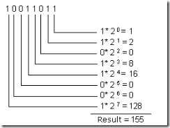
As you can see, converting a binary number into a decimal number is done by calculating the expression on the left side. Depending on the position in a binary number, digits carry different values which are multiplied by themselves, and by adding them we get a decimal number we can understand. Let's further suppose that there are few marbles in each of the drawers: 2 in the first one, 4 in the second drawer, 7 in the third and 3 in the fourth drawer. Let's also say to the one who's opening the drawers to use binary representation in answer. Under these conditions, question would be as follows: "How many marbles are there in 01?", and the answer would be: "There are 100 marbles in 01." It should be noted that both question and the answer are very clear even though we did not use the standard terms. It should further be noted that for decimal numbers from 0 to 3 it is enough to have two binary digits, and that for all values above that we must add new binary digits. So, for numbers from 0 to 7 it is enough to have three digits, for numbers from 0 to 15, four, etc. Simply said, the biggest number that can be represented by a binary digit is the one obtained when basis 2 is graded onto a number of binary digits in a binary number and thus obtained number is decremented by one.
Example:
This means that it is possible to represent decimal numbers from 0 to 15 with 4 binary digits, including numbers '0' and '15', or 16 different values.
Operations which exist in decimal numerical system also exist in a binary system. For reasons of clarity and legibility, we will review addition and subtraction only in this chapter.
Basic rules that apply to binary addition are:

Addition is done so that digits in the same numerical positions are added, similar to the decimal numerical system. If both digits being added are zero, their sum remains zero, and if they are '0' and '1', result is '1'. The sum of two ones gives two, in binary representation it will be a zero, but with transferring '1' to a higher position that is added to digits from that position.
Example:

We can check whether result is correct by transferring these number to decimal numerical system and by performing addition in it. With a transfer we get a value 10 as the first number, value 9 as the second, and value 19 as the sum. Thus we have proven that operation was done correctly. Trouble comes when sum is greater than what can be represented by a binary number with a given number of binary digits. Different solutions can be applied then, one of which is expanding the number of binary digits in the sum as in the previous example.
Subtraction, like addition is done on the same principle. The result of subtraction between two zeros, or two ones remains a zero. When subtracting one from zero, we have to borrow one from binary digit which has a higher value in the binary number.
Example:

By checking the result as we did with addition, when we translate these binary numbers we get decimal numbers 10 and 9. Their difference corresponds to number 1 which is what we get in subtraction.
B.3 Hexadecimal numerical system
Hexadecimal numerical system has a number 16 as its basis. Since the basis of a numerical system is 16, there are 16 different digits that can be found in a hexadecimal number. Those digits are "0, 1, 2, 3, 4, 5, 6, 7, 8, 9, A, B, C, D, E, F". Letters A, B, C, D, E and F are nothing but values 10, 11, 12, 13, 14 and 15. They are introduced as a replacement to make writing easier. As with a binary system, here too, we can determine with same formula what is the biggest decimal number we can represent with a specific number of hexadecimal digits.
Example: With two hexadecimal digits
Usually, hexadecimal number is written with a prefix "$" or "0x" ,or suffix"h" , to emphasize the numerical system. Thus, number A37E would be written more correctly as $A37E, 0xA37E, or A37Eh. In order to translate a hexadecimal number into a binary numerical system it is not necessary to perform any calculation but simple exchange of hexadecimal digits with binary digits. Since the maximum value of a hexadecimal number is 15, that means that it is enough to use 4 binary digits for one hexadecimal digit.
Example:

By checking, that is transferring both numbers into decimal numerical system, we get a number 228 which proves the accuracy of our action.
In order to get a decimal equivalent of a hexadecimal number, we need to multiply each digit of a number with number 16 which is gradated by the position of that digit in hexadecimal number.
Example:

Addition is, like in two preceding examples, performed in a similar manner.
Example:

We need to add corresponding number digits. If their sum is equal 16, write 0 and transfer one to the next higher place. If their sum is greater than 16, write value above and transfer 1 to the next higher digit.Eg. if sum is 19 (19=16+3) write 3 and transfer 1 to the next higher place. By checking, we get 14891 as the first number, and second is 43457. Their sum is 58348, which is a number $E3EC when it is transferred into a decimal numerical system. Subtraction is an identical process to those in previous two numerical systems. If the number we are subtracting is smaller, we borrow from the next place of higher value.
Example:

By checking this result, we get values 11590 for the first number and 5970 for the second, where their difference is 5620, which corresponds to a number $15F4 after a transfer into a decimal numerical system.
Conclusion
Binary numerical system is still the one that is most in use, decimal the one that's easiest to understand, and a hexadecimal is somewhere between those two systems. It's easy conversion to a binary numerical system and easy memorization make it, along with binary and decimal systems, one of the most important numerical systems.
Introduction
- Microcontroller
- I/O pin
- Software
- Hardware
- Simulator
- ICE
- EPROM Emulator
- Assembler
- HEX file
- List file
- Source File
- Debugging
- ROM, EPROM, EEPROM, FLASH, RAM
- Addressing
- ASCII
- Carry
- Code
- Byte, Kilobyte, Megabyte
- Flag
- Interrupt vector or interrupts
- Programmer
- Product
Since all the fields of man's activity are regularly based on adequate and already adopted terms (through which other notions and definitions become), so in the field of microcontrollers we can single out some frequently used terms. Ideas are often connected so that correct understanding of one notion is needed in order to get acquainted with one or more of the other ideas.
Microcontroller Microprocessor with peripherals in one electronic component. I/O pin External microcontroller's connector pin which can be configured as input or output. In most cases I/O pin enables a microcontroller to communicate, control or read information. Software Information that microcontroller needs in order to be able to function. Software can not have any errors if we want the program and a device to function properly. Software can be written in different languages such as: Basic, C, pascal or assembler. Physically, that is a file on computer disc. Hardware Microcontroller, memory, supply, signal circuits and all components connected with microcontroller. The other way of viewing this (especially if it's not working) is, that, hardware is something you can kick. Simulator Software package for PC which simulates the internal function of microcontroller. It is ideal for checking software routines and all the parts of the code which do not have over demanding connections with an outside world. Options are installed to watch the code, movement around the program back and forth step by step, and debugging. ICE ICE (In Circuit Emulator), internal emulator, very useful part of the equipment which connects a PC instead of microcontroller on a device that is being developed. It enables software to function on the PC computer, but to appear as if a real microcontroller exists in the device. ICE enables you to move through program in real time, to see what is going on in the microcontroller and how it communicates with an outside world. EPROM Emulator EPROM Emulator is a device which does not emulate the entire microcontroller like ICE emulator, but it only emulates its memory. It is mostly used in microcontrollers that have external memory. By using it we avoid constant erasing and writing of EPROM memory. Assembler Software package which translates source code into a code which microcontroller can understand. It contains a section for discovering errors. This part is used when we debug a program from errors made when program was written. HEX file This is a file made by assembler translator when translating a source file, and has a form "understood" by microcontrollers. A continuation of the file is usually File_name.HEX where the name HEX file comes from. List file This is a file made by assembler translator and it contains all instructions from source file with addresses and comments programmer has written. This is a very useful file for keeping track of errors in the program. File extension is LST which is where its name comes from. Source File File written in the language understood by man and assembler translator. By translating the source file, we get HEX and LIST files. Debugging Error made in writing a program, which error we are not aware of. Errors can be quite simple such as typing errors, and quite complex such as incorrect use of program language. Assembler will find most of these errors and report them to '.LST' file. Other errors will need to be searched for by trying it out and watching how device functions. ROM, EPROM, EEPROM, FLASH, RAM Types of memories we meet with microcontroller use. First one can not be erased, what you write in it once, stays forever, and can not be erased. The second is erasable with UV lamp. Third one can be erased electrically, using voltage which microcontroller operates on. Fourth one is electrically erasable, but unlike EEPROM memory it does not have such a great number of cycles of writing and erasing at memory locations. Fifth one is fast, but it does not hold back the contents as the previous when there is supply shortage. Thus, program is not stored in it, but it serves for different variables and inter-results. Addressing Determines and designates certain memory locations. ASCII Short for "American Standard Code for Information Interchange". It is widely accepted type of coding where each number and letter have their eight-bit code. Carry Transfer bit connected with arithmetic operations Code File, or section of a file which contains program instructions. Byte, Kilobyte, Megabyte Terms designating amounts of information. The basic unit is a byte, and it has 8 bits. Kilobyte has 1024 bytes, and mega byte has 1024 kilobytes. Flag Bits from a status register. By their activation, programmer is informed about certain actions. Program activates its response if necessary. Interrupt vector or interrupts Location in microcontroller memory. Microcontroller takes from this location information about a section of the program that is to be executed as an answer to some event of interest to programmer and device. Programmer Device which makes it possible to write software in microcontroller memory, thus enabling the microcontroller to work independently. It consists of the hardware section usually connected with one of the ports and software section used on the computer as a program. Product Product development is a combination of luck and experience. Short terms, or time-limits for production should be avoided because even with most simple assignments, much time is needed to develop and improve. When creating a project, we need time, quiet, logical mind and most importantly, a thorough understanding of consumer's needs. Typical course in creating a product would have the following algorithm.

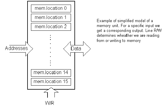
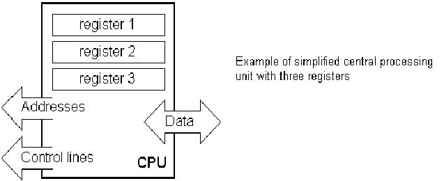
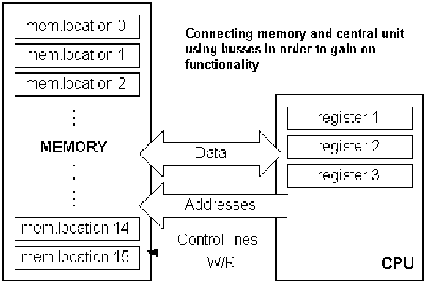
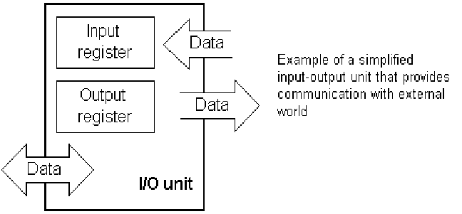


![clip_image002[4] clip_image002[4]](https://blogger.googleusercontent.com/img/b/R29vZ2xl/AVvXsEiiuxnidbsNqFmNwR8uOsD2b5r3x3P7EQ_3akbXFiwzHwneU5MuXchE0jGeLY9c31eBRZxAzwVuICt5roanTsb-Ex4lDgEgMX1izoxohwoPc_vgLdpRrF3KMXtuNfUdOKGSiNyrf75_1M0/?imgmax=800)


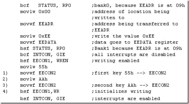
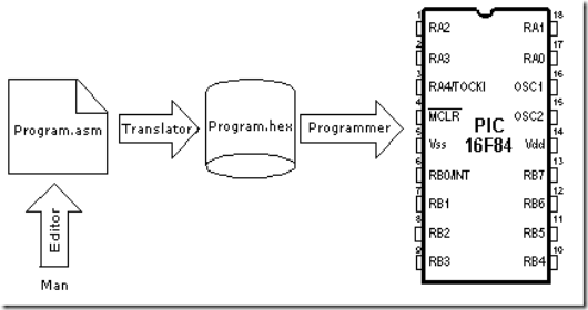
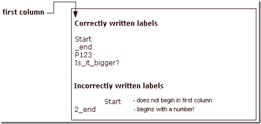


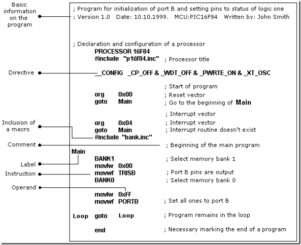


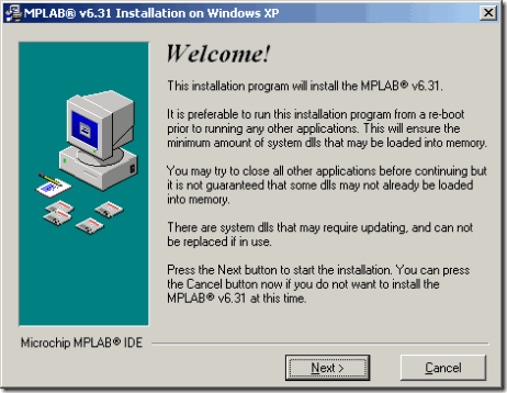


![clip_image005[1] clip_image005[1]](https://blogger.googleusercontent.com/img/b/R29vZ2xl/AVvXsEjX9WTSN8FOk9KRzlKSR0JRzvXdqtdkatBouBRrCjSaDJDyPAvqL-u6a5JY1IIEeIXC936w2ZQE62M19H6EkSEi-TWJuZtW0ImO8Z2azTK7nOnLehhOagUd-OYPRJhvuqZ3rXWxEvhqMOg/?imgmax=800)


