Manufacturing of Integrated Circuits
Semiconductor Processing Basics
All mainstream semiconductor integrated-circuit processes start with a thin slice of silicon, known as a substrate or wafer. This wafer is circular and ranges from 4 to 18 inches in diameter and is approximately 1 mm thick (hence its name). Each wafer is cut from a single crystal of the element silicon and polished to its final thickness with atomic smoothness. Most circuit designs (like your processor) fit into a few square centimeters of silicon area; each self-contained area is known as a die. After fabrication, the wafer is cut to produce independent, rectangular dies often known as chips, which are then packaged to produce the final component you buy at the store.


A specific sequence or process of chemical and mechanical modifications is performed on certain areas of the wafer. Although complex processes employ a variety of techniques, a basic IC process will employ one of the following three modifications to the wafer:
• Implantation: Atoms or molecules are added to the silicon wafer, changing its electronic properties
• Deposition: Materials such as metals, insulators, or semiconductors are added in thin layers (like painting) on to the wafer
• Etching: Material is removed from the wafer through chemical reactions or mechanical motion
Lithography
When building a multi-component IC, we need to perform different modifications to differents areas of the wafer. We may want to etch some areas and add metal to others, for example. The method by which we define which areas will be modified is known as lithography.
Lithography has evolved much over the last 40 years and will continue to do so. Modern lithography employs all of the basic principles described below, but uses complex computation, specialized materials, and optical devices to achieve the very high resolutions required to reach modern feature sizes.
At its heart, lithography is simply a stencil process. In an old-fashioned stencil process, when a plastic sheet with cut-out letters or numbers is laid on a flat surface and painted, only the cutout areas would be painted. Once the stencil is removed, the design left behind consists of only the painted areas with clean edges and a uniform surface. With that in mind.Given a flat wafer, we first apply a thin coating of liquid polymer known as photoresist (PR). This layer usually is several hundred nanometers thick and is applied by placing a drop in the center of the wafer and then spinning the wafer very fast (1000 to 5000 rpm) so that the drop spreads out evenly over the surface. Oncecoated, the PR is heated (usually between 60 to 100◦C) in a process known as baking; this allows the PR to solidify

slightly to a plastic-like consistency. Once baked and when exposed to ultraviolet (UV) light, the bonds that hold the PR molecules together are "chopped" up; this makes it easy to wash away the UV-exposed areas (some varieties of PR behave in exactly the opposite manner: UV light makes the PR very strong or cross-linked, but we will ignore that technique here). In lithography, UV light is focused through a glass plate with patterns on it; this is known as exposure. These patterns act as a "light stencil" for the PR. Wherever UV light hits the PR, that area subsequently can be washed away in a process called development. After development, the PR film remains behind with holes in certain areas.
How is this helpful? Let's look at how the modifications presented earlier can be masked with PR to produce patterned effects. In each case, we first use lithography to pattern areas onto the wafer then we perform one of our three processes and finally, we use a strong solvent such as acetone (nail polish remover) to completely wash away the PR . The PR allows us to implant, deposit, or etch only in defined areas.
Fabricating a Diode
We discussed the functional performance of the diode as a circuit component. Here, we will examine briefly how a diode is fabricated. Similar but more complex multi-step processes are used to make transistors and integrated circuits. Conceptually, the simplest diode is made from two slabs of silicon—each implanted with different atoms—pressed together such that they share a boundary. The n and p areas are pieces of silicon that have been implanted with atoms (known as impurities) that increase or decrease the number of electrons capable of flowing freely through the silicon.


Wires are made by depositing metal layers on top of the device; these are called interconnects. Modern ICs have 6 to 7 such interconnect layers. These layers are used to make electrical connections between all of the various components in the IC in the same way that macroscopic wires are used to link components on a breadboard


Three-dimensional integrated circuits (3DICs) have attracted attention in industry and academia as it may provide an enabling technology that relaxes today's interconnect-bottleneck. As device densities continue to increase with advances in lithography and device design, device-to-device interconnects will continue to be a major design issue. The ITRS 99 roadmap projects that the
number of metal layers at the 50-nm generation will be 9-10. With current manufacturing technologies, it will be a major challenge for future designs to be able to manage such complexity while maintaining the performance improvements that the market demands. Multi-layer device structures such as 3D-ICs, are seen as a possible solution for this challenge.
It can be shown that 3-D architectures can reduce the overall global and semi-global wire-length, while increasing the number of local wires. Moreover, the decrease in the number of long interconnects could directly translate to an increase in device density, provided that the devices are efficiently packed, placed, and wired. In addition to these potential benefits, the 3-D architecture lends itself to the realization of a "system-on-a-chip." Monolithic mixed-technology options, such as 3-D Imagers, have already shown promise .Other opportunities, such as OEIC-on-Si technology, memory on- logic, and various microelectromechanical (MEMS) hybrids are also possible. There exist a plethora of 3-D integration techniques in literature, but the two most appealing and competitive schemes to date are those involving either low temperature silicon epitaxy or wafer bonding. The central theme between these two methods is vertical integration - namely, the addition of CMOS devices on top of each other. Their inherent differences, however, are of course the stacking technique itself, as well as each scheme's potential for high vertical connectivity and "system-on-a-chip" integration. For instance, in the epitaxy scheme, multiple device layers can be realized by repeating the "Si epitaxy followed by a CMOS flow" cycle", where successive device layers are fabricated in serial mode. The enabling technology is a well-characterized low-temperature Si epitaxy, which is crucial for thermal budget minimization of the process flow. Layer-to-layer connections can made from either inter-layer vias or from direct source-drain / source-drain contacts using sandwiched polysilicon lines. In theory, the combination of Si epitaxy with local poly-Si interconnects would probably create a true 3-D system, where it will contain the highest vertical
connectivity of all current 3-D schemes. But 3-D integration with serial Si epitaxy comes with a price: It will be very difficult to implement circuit integration with mixed-technologies (i.e. III-V optics with CMOS). On the other hand, in the wafer bonding approach, integration of mixed technologies is of second nature. In most wafer bonding schemes, multiple device wafers in the stack are held together with adhesives (i.e. polymers, metal-to-metal thermo compression, low-melting point eutectic solders, etc.), and inter-layer vias provide layer-to-layer communication. Although the process flows do vary significantly, most wafer bonding schemes share four common considerations: a) The bonding medium ("glue") of choice, b) If needed, a method for Si substrate thinning, c) The wafer-to-wafer alignment accuracy, and d) The inter-layer electrical interconnection method. To be specific, the remainder of this paper will focus on these considerations that apply to 3-D integration with Cu-Cu Wafer bonding.
Process Flow
In our 3-D integration scheme, multiple device wafers are sequentially bonded to each other using low temperature Cu-Cu thermo compression. Figure 1depicts our definition of a 3-D circuit, in which two device layers are both bonded and electrically interconnected using Cu-Cu pads (the bonding interface).

The ideal case for such architecture is to have the smallest possible lateral dimensions for the Cu pads and inter-wafer vias to ensure high via density. In reality, wafer-wafer alignment tolerances during bonding and the maximum aspect ratio of the vias one can create will ultimately be the size-limiting determinants of these vias / Cu pads .As shown in Figure 1, when
the top device layer is a thin SOI, the aspect ratio of the inter-wafer vias can be relaxed to around 3:1 or even 2:1 for ease in fabrication, while still maintaining a relatively high vertical density across the wafer. To recapitulate, the goal of our process flow is to create a 3-D stack by successive bonding of SOI device layers on top of each other. Figure 2 is a flowchart of such
a process, in which the 3-D stack begins with bonding of two device wafers, and subsequent device layers can be added to the stack in a short turn-around process loop. As seen in this chart, the majority of the processing steps revolve around the preparation of the first SOI substrate
prior to bonding (mainly for substrate thinning), which is the focus of the next three subsections.

Handle Wafer Attachment
Our 3-D scheme begins with a typical SOI substrate (100 nm SOI / 400 nm BOX) that contains both CMOS devices and its corresponding multilevel interconnects - essentially a "finished" circuit. Next, in order to stack this SOI on top of another device layer, it first has to undergo
backside substrate thinning. For mechanical support during grindback, it is imperative to attach the SOI to a handle wafer with a special adhesive that is: a) Strong enough to withstand vigorous shearing force from grinding, Chemically inert to hot aqueous hydroxide solutions Can easily be removed with another solution.
Because hot basic solutions will usually delaminate organic polymers from their substrates, it is very difficult for CMOS-compatible polymer adhesives to satisfy all three criteria. However, these requirements can be met with a careful choice of metallic bonding layers; hence,
one can use a Cu-Cu bond as the adhesion layer itself, while flanking layers of Zr can be used as the "wafer release" medium. This is due to the fact that Cu generally resists hydroxide attack, and Zr dissolves extremely rapidly in dilute HF (much faster than SiO2). The complete handle wafer attachment scheme

To begin with, (300 / 50) nm thick Cu/Ta contact pads are patterned on top of the SOI substrates, which is then passivated by an overlayer of 500 nm PECVD oxide and followed by oxide CMP for global planarization. These Cu pads, with lateral dimensions on the order of 3-5 μm, are inconsequential in handle wafer bonding, but will eventually participate in device-device wafer bonding. Once passivated and planarized, the SOI substrate is ready for handle wafer attachment. On both the SOI substrate and the 100 nm LPCVD nitride handle wafer, 150 nm Zr and 300 nm Cu was deposited in sequence. With no need for wafer-wafer alignment, the SOI and the nitride handler were bonded at 40 oC in N2 ambient with persistent contact pressure of 4000 mbar for 30 min. The pair underwent a further anneal at 400oC in N2, in which the Cu-Cu interface forms a strong bond that passes both the razor test [and subsequent mechanical substrate.
Substrate Etch back and Backside Via Formation
With the handle wafer in place, the next task involves the complete removal of the SOI bulk Si using a combination of mechanical grind back and aqueous chemical etching, which will selectively stop on the 400 nm buried oxide (BOX) layer.

To start, 400-420 μm of the SOI bulk was removed using grinding, while the remaining 80 to 100 μm of Si was etched in a solution containing 4.38 M (20% wt) KOH at 80oC for approximately 2 hrs, which has a Si-to-oxide selectivity of about 300 : 1. In addition, at the same KOH concentration, Zr is virtually impervious to hydroxide attack until the solution temperature reaches beyond 120oC. Last, but not least, the 100 nm LPCVD nitride layer provides a near-perfect protection of the handle wafer against KOH attack. Although Cu has excellent corrosion resistant to alkaline (except for ammonia and other Cu chelates) solutions of all concentrations at room temperature, the metal will undergo some oxidation at environments above 50-60oC. With our 4.38 M KOH solution at 80oC, we have observed spurious spots of Cu-Cu interface
delamination at the wafer edges. This delamination situation seems to be ubiquitous - it also occurs in TMAH (tetramethylammonium hydroxide) or EDP (ethylenediamine with 1,2-benzenediol and water) etches of similar concentration and temperature [8,9] There are two ways to prevent such Cu corrosion: One can either reduce the exposure time to hydroxide attack, or one can add a Cu corrosion inhibitor to the etch solution. Currently, we can completely suppress Cu-Cu interface corrosion by adding 0.025 M tolyltriazole (C7H6N3, monopotassium salt) without sacrificing the Sito-oxide selectivity, but at the expense of a 10 μm/hr decrease in the Si etch rate.upon completion of SOI substrate removal, inter-layer vias are created by etching through the BOX, SOI, and ILD 1, finally stopping on metal layer M1. This is followed by PECVD oxide sidewall passivation and via filling using a damascene process.A typical via aspect ratio is around 2:1, with a via width about 0.5 μm.

Finally, (300 / 50 nm) thick Cu/Ta pads, with lateral dimensions on the order of 3 to 5 μm, are patterned right on top of the inter-layer vias. Auxiliary Cu pads, which has no role in inter-wafer communication, can also be patterned to increase the total surface area for subsequent Cu-Cu wafer bonding.
Wafer-Wafer Alignment and Bonding
The thinned SOI substrate in the picture, complete with backside inter-layer vias and Cu bond pads, is now ready to be bonded to another CMOS device wafer, presumably also with its own set of multilevel interconnects and Cu/Ta bond pads that mirror those of the thinned SOI.
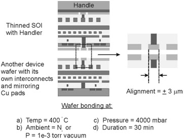
Both wafer-to-wafer alignment and bonding were performed in the Electronic Vision EV 450 Aligner and AB1-PV Bonder [5,7]. Since the system has an inherent + 3 μm mis-alignment, any Cu/Ta bond pads less than or equal to 3 μm are unacceptable. Thus, wafer-to-wafer
alignment is the ultimate factor in determining the interlayer via density. With better optical alignment systems, it is possible to decrease the Cu/Ta pad sizes down to around 0.5 to 1 μm, which corresponds to a substantial increase in via density. When the wafers were properly aligned, the pair was clamped and transferred to the bonding chamber, where both substrates were heated to 400oC in N2 ambient and hot-pressed for 30 min under 4000 mbar of pressure.
Further anneal at 400oC for 30 min in N2 completes the Cu-Cu bond.
Handle Wafer Release
The final step of our 3-D integration scheme is releasing the handle wafer from the top SOI layer.

higher than the rate of SiO2 degradation. With vigorous agitation, Zr undercutting across the whole wafer can occur in about 10 to 15min, thereby releasing the nitride handler from the finished 3-D stack. Further dipping of the 3-D stack in dilute HF will expose the Cu/Ta bond
pads created earlier in Section 2.1. On a side-note, Ti was not used as the release layer because it is rigorously attacked by KOH around and above 80oC. Now, the finished 3-D stack, with the Cu/Ta pads exposed, can immediately be bonded to another thinned SOI, and thus exhibiting the parallelism, process repeatability and robustness of this 3-D integration scheme.
Circuit-Design Tools for 3-D Integration
No circuit fabrication technology is commercially viable without tools that allow designers to develop circuits using the technology. A number of tools have been developed or are in progress that can be used, for example, to generate masks, or to take a higher-level schematic and target it for fabrication in 3-D. As this technology matures, the ongoing work in this area will ensure that circuit designers are capable of utilizing the advantages 3-D has to offer